Display device and driving method thereof

A technology of a display device and a driving method, which is applied to static indicators, instruments, etc., and can solve the problems of sub-pixel 20 brightness degradation, short charging time, insufficient charging, etc.

Inactive Publication Date: 2011-05-11
AU OPTRONICS CORP
View PDF0 Cites 6 Cited by
  • Summary
  • Abstract
  • Description
  • Claims
  • Application Information

AI Technical Summary

Problems solved by technology

Due to the short charging time of the sub-pixel 20, it is prone to undercharging
Experiments have also proved that the sub-pixel 20 will experience a serious decline in brightness when operated at high frequencies.
Therefore, a

Method used


Image

  • Display device and driving method thereof
  • Display device and driving method thereof
  • Display device and driving method thereof

Examples


no. 1 example

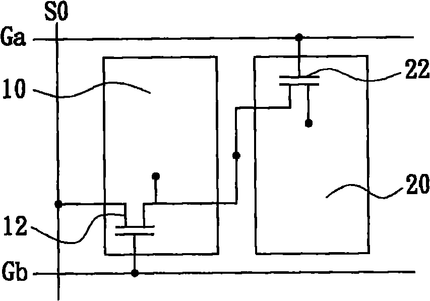
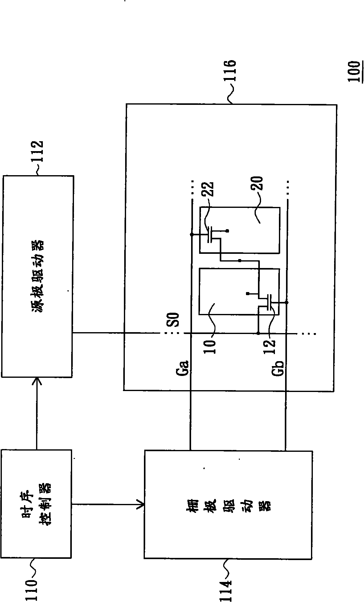
[0026] see image 3 , which is an explanatory diagram of a display device according to an embodiment of the present invention. As shown in the figure, the display device 100 of the present invention includes a timing controller 110 , a source driver 112 , a gate driver 114 and a display panel 116 . The timing controller 110 is electrically coupled to the source driver 112 and the gate driver 114 , and both the source driver 112 and the gate driver 114 are electrically coupled to the display panel 116 . The timing controller 110 is used to control the operation of the source driver 112 and the gate driver 114 , so as to control the display panel 116 to display desired images through the source driver 112 and the gate driver 114 . The above-mentioned display panel 116 further includes a scan line Ga, a scan line Gb, a signal line S0 , sub-pixels 10 , sub-pixels 20 , transistors 12 and transistors 22 . The gate of the transistor 12 is electrically coupled to the gate driver 114...

no. 2 example

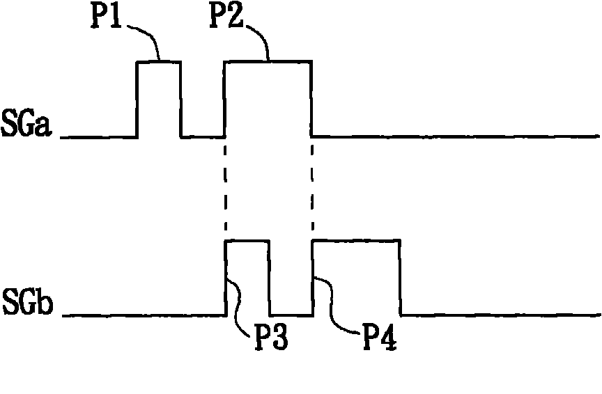
[0031] by Figure 4 It can be seen from its corresponding description that as long as the pulse enable periods of the pulses P4 and P2 overlap at least partially, and the pulse enable periods of the pulse P5 and pulse P3 overlap at least partially, the sub-pixel 20 can obtain a second charging opportunity . Therefore, in the second embodiment, the rising edge of the pulse P4 is at the same time point as the rising edge of the pulse P2, and the falling edge of the pulse P4 is at the same time point as the falling edge of the pulse P2.

no. 3 example

[0033] According to the discussion of the second embodiment, in this embodiment, the Figure 4 The rising edge of the pulse P4 is between the falling edge of the pulse P1 and the rising edge of the pulse P2, and the falling edge of the pulse P4 is between the falling edge of the pulse P2 and the rising edge of the pulse P3.


PUM


Abstract

The invention provides a display device and a driving method thereof. The display device comprises a first scanning line, a second scanning line, a signal line, a first sub-pixel, a second sub-pixel, a first transistor, a second transistor and a gate driver, wherein a gate of the first transistor is coupled with the second scanning line; one source/drain of the first transistor is coupled with the signal line, and the other source/drain of the first transistor is coupled with the first sub-pixel; a gate of the second transistor is coupled with the first scanning line; one source/drain of the second transistor is coupled with the other source/drain of the first transistor, and the other source/drain of the second transistor is coupled with the second sub-pixel; the gate driver is coupled with the first scanning line and the second scanning line, is used for providing the first pulse, the second pulse and the third pulse to the first scanning line in sequence and is also used for providing the fourth pulse, the fifth pulse and the sixth pulse to the second scanning line in sequence; at least parts of the fifth pulse and third pulse overlap during the enabling period; and at least parts of the fourth pulse and second pulse overlap during the enabling period.

Description

technical field [0001] The present invention relates to a display device, in particular to a display device with relatively sufficient charging time of sub-pixels and a driving method thereof. Background technique [0002] With the continuous development of display technology, at present, liquid crystal display (Liquid Crystal Display, LCD) has gradually replaced the traditional cathode ray display (Cathode Ray Tube, CRT) because of its advantages of small size and light weight, and is widely used by the society. It is widely used by the public, especially in electronic products such as monitors, notebook computers, digital cameras and projectors. Since electronic products tend to be lighter, thinner, shorter, and smaller, the industry has developed a semi-data-driven (HSD2) technology applied to liquid crystal display panels to further reduce the volume of liquid crystal displays. The so-called half-data driving technology is a design in which one signal line is used to se...

Claims


Application Information

Patent Timeline
IPC IPC(8): G09G3/36
Inventor 陈昱丞王士豪王参群罗婉瑜陈茂松
Owner AU OPTRONICS CORP
Why Eureka
Try Eureka