
Static discharge protection device

A technology of electrostatic discharge protection and well resistance, which is applied in the field of electrostatic discharge protection devices, can solve the problems that are not suitable for high-frequency applications and analog circuit applications, and the area occupied by electrostatic discharge protection devices is large, so as to achieve good conduction uniformity Effect

Active Publication Date: 2012-08-01
STATE GRID CORP OF CHINA +2
View PDF0 Cites 0 Cited by
  • Summary
  • Abstract
  • Description
  • Claims
  • Application Information

AI Technical Summary

Problems solved by technology

[0011] The invention solves the problem that the prior art electrostatic discharge protection device occupies a relatively large area and is not suitable for some high-frequency applications and analog circuit applications

Method used


Image

  • Static discharge protection device
  • Static discharge protection device
  • Static discharge protection device

Examples


Embodiment Construction

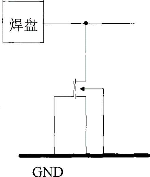
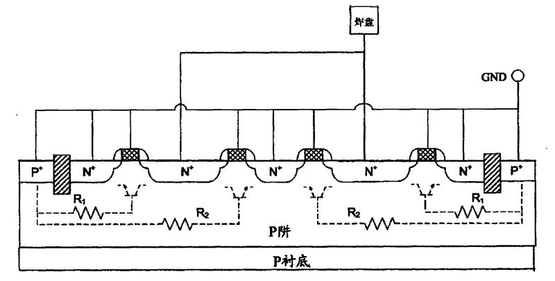
[0023] From the description of the aforementioned prior art, it can be found that for an electrostatic discharge protection device composed of multiple parallel-connected gate-grounded NMOS transistors, since the positions of each NMOS transistor are different, it will inevitably cause the base of the parasitic NPN transistor corresponding to each NMOS transistor The resistors are also different. According to the foregoing analysis, it is inevitable that the parasitic NPN transistor corresponding to the NMOS transistor whose gate is grounded in the middle position is turned on first. In view of this, if the NMOS transistor whose gate is grounded first can be used to provide an external current similar to the leakage current mentioned above to the substrate, it will help to turn on the parasitic NPN transistors corresponding to other NMOS transistors.

[0024] Based on this design concept, an embodiment of the electrostatic discharge protection device of the present invention i...


PUM


Abstract

The invention provides a static discharge protection device, comprising a plurality of NMOS pipes which are connected in parallel and are formed within the same deep trench and are grounded by means of the grid electrodes, wherein the drain electrode of each NMOS pipe is connected to a bonding pad, the source electrode and the base electrode of at least one NMOS pipe which is arranged on the central position are connected and are grounded by means of trench resistance. The base electrodes and source electrodes of other NMOS pipes are grounded. The static discharge protection device provided by the invention has the advantages that the conduction uniformity is good, the area is saved and the static discharge protection device is more suitable for high frequency application and analogue circuit application and etc.

Description

technical field [0001] The invention relates to the field of semiconductor integrated circuit design, in particular to an electrostatic discharge protection device. Background technique [0002] As the functions of semiconductor devices become increasingly complex and their sizes decrease, the upper limit of the electrostatic discharge (ESD, Electro Static Discharge) voltage that they can withstand is also decreasing. Therefore, the adverse effects of electrostatic discharge on semiconductor devices are becoming more and more serious. [0003] In the existing design of ESD protection, specially designed NMOS transistors are often used to form an ESD protection device. For example, an NMOS transistor with a gate ground (Gate Ground) is used as an ESD device to form an ESD protection device. [0004] For example, combining figure 1 and figure 2 As shown, for the case where multiple parallel gate-grounded NMOS transistors are used for electrostatic discharge protection, eac...

Claims


Application Information

Patent Timeline
Patent Type & Authority Patents(China)
IPC IPC(8): H01L27/088H01L23/60H02H9/00
Inventor 单毅
Owner STATE GRID CORP OF CHINA
Learn More