Unlock instant, AI-driven research and patent intelligence for your innovation.
A ldmos‑scr device with source-side embedded interdigitated nmos
What is Al technical title?
Al technical title is built by PatSnap Al team. It summarizes the technical point description of the patent document.
A technology of LDMOS-SCR and devices, which is applied in the direction of electric solid-state devices, semiconductor devices, semiconductor/solid-state device components, etc., can solve the problems of insufficient anti-latch-up ability and low maintenance voltage, and achieve the purpose of increasing ESD current discharge capacity , Enhance the coupling effect of resistance and capacitance, and improve the effect of ESD robustness
Active Publication Date: 2018-01-02
JIANGNAN UNIV
View PDF5 Cites 0 Cited by
Summary
Abstract
Description
Claims
Application Information
AI Technical Summary
This helps you quickly interpret patents by identifying the three key elements:
Problems solved by technology
Method used
Benefits of technology
Problems solved by technology
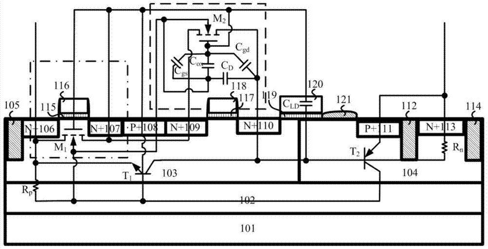
[0004] In view of the common problems of low maintenance voltage and insufficient anti-latch-up ability of the existing ESD protection devices with SCR structure, the present invention designs an LDMOS-SCR device with interdigitated NMOS embedded in the source end, which not only makes full use of the SCR The device is characterized by strong robustness, and the resistance-capacitance coupling effect formed by the increased N+ implantation region at the source of the device, the polysilicon gate and the thin gate oxide layer is used to improve the maintenance voltage of the ESD protection design scheme and enhance the ESD robustness of the device sex
Method used
Image
Click on the blue label to locate the original text in one second.
Reading with bidirectional positioning of images and text.
Examples
Embodiment Construction
[0025] Below in conjunction with accompanying drawing and specific embodiment the present invention will be described in further detail:
[0026] The example of the present invention designs an LDMOS-SCR device with interdigitated NMOS embedded in the source terminal, which not only utilizes the high-voltage resistance characteristics of LDMOS, but also utilizes the robustness of SCR strong ESD current. The interdigitated NMOS structure is embedded in the terminal design, and the resistance-capacitance coupling effect is formed by means of the source-side substrate parasitic resistance to improve the current conduction uniformity and turn-on speed of the device, enhance the ESD robustness of the device, and also increase the size of the device. the sustaining voltage.
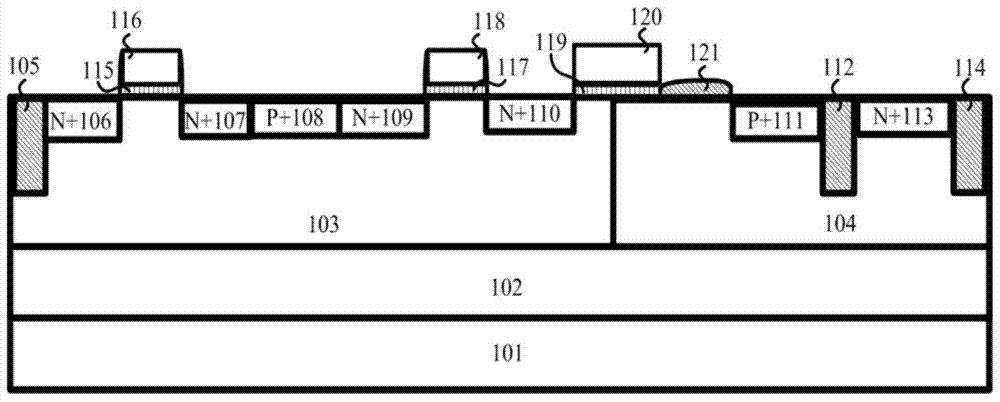
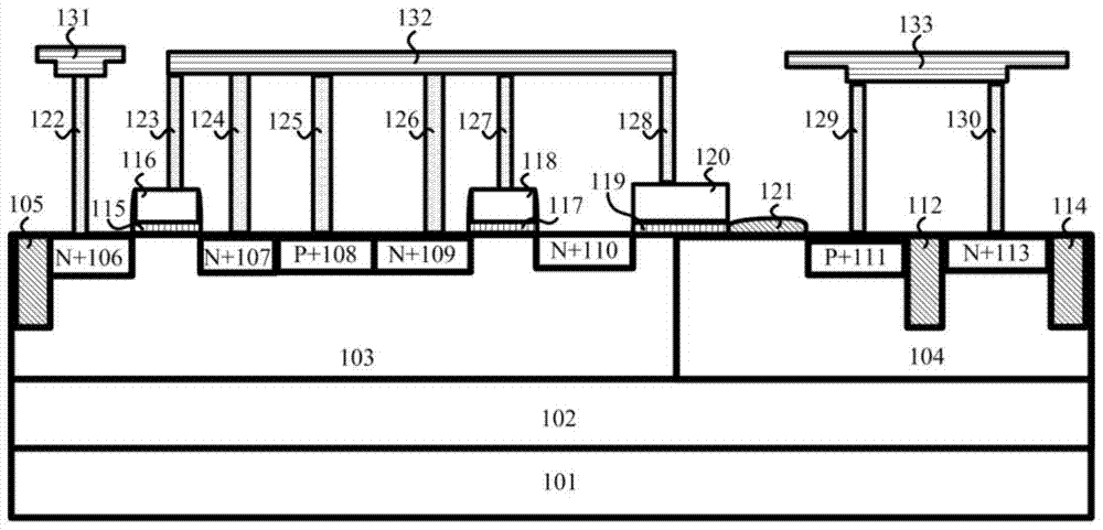
[0027] Such as figure 1 The sectional view of the internal structure of the example device of the present invention shown, its main feature is: mainly by P substrate 101, P epitaxy 102, P well 103, N well 104,...
PUM
Abstract
An LDMOS‑SCR device with source-side embedded interdigitated NMOS for improved ESD protection reliability of on-chip ICs. Mainly composed of P substrate, P epitaxy, P well, N well, first N+ implantation region, second N+ implantation region, first P+ implantation region, third N+ implantation region, fourth N+ implantation region, second P+ implantation region , the fifth N+ implantation region, a plurality of polysilicon gates, a plurality of thin gate oxide layers and a plurality of field oxygen isolation regions. On the one hand, the device forms a parasitic LDMOS-SCR current path by the second P+ injection region, the third polysilicon gate, the fifth N+ injection region, the N well, the P well, the first P+ injection region, and the first N+ injection region. The ESD robustness of the device can be enhanced; on the other hand, the first N+ implantation region, the first polysilicon gate, the first thin gate oxide layer, the second N+ implantation region, the first P+ implantation region, and the third N+ implantation region The interdigitated NMOS and parasitic resistance formed by the second polysilicon gate, the second thin gate oxide layer and the fourth N+ implantation region can form a resistance-capacitance coupling effect and increase the sustaining voltage.
Description
technical field [0001] The invention belongs to the field of electrostatic discharge protection of integrated circuits and relates to an ESD protection device, in particular to an ESD protection device with an LDMOS-SCR embedded with interdigitated NMOS at the source end, which can be used to improve the reliability of ESD protection of ICs on a chip . Background technique [0002] ESD (electrostatic discharge) is one of the important factors affecting the reliability of today's IC. Circuit dysfunction or gate oxide breakdown damage caused by ESD to ICs has attracted widespread attention in the industry. The damage phenomenon caused by ESD in IC is mainly manifested in the following aspects: dielectric breakdown caused by ESD in semiconductor devices, resulting in rupture of oxide film; local overheating of internal circuits caused by EOS (electrical overstress) or ESD in IC , leading to the melting of metal wires; in ESD protection devices, due to the low voltage clamping...
Claims
Application Information
Patent Timeline
Application Date:The date an application was filed.
Publication Date:The date a patent or application was officially published.
First Publication Date:The earliest publication date of a patent with the same application number.
Issue Date:Publication date of the patent grant document.
PCT Entry Date:The Entry date of PCT National Phase.
Estimated Expiry Date:The statutory expiry date of a patent right according to the Patent Law, and it is the longest term of protection that the patent right can achieve without the termination of the patent right due to other reasons(Term extension factor has been taken into account ).
Invalid Date:Actual expiry date is based on effective date or publication date of legal transaction data of invalid patent.

