Method for checking electric fitting data of printed circuit board

A printed circuit board and printed circuit technology, applied in the computer field, can solve the problems of no assembly review, inability to directly extract assembly information, and no data storage format, so as to improve research and production efficiency and shorten design cycle. , the effect of saving design time and materials

Inactive Publication Date: 2011-05-25
XIDIAN UNIV
View PDF2 Cites 33 Cited by
  • Summary
  • Abstract
  • Description
  • Claims
  • Application Information

AI Technical Summary

Problems solved by technology

However, there are many types of electronic design automation EDA design software on the market at present, and the PCB design results are generally saved in the format of each EDA software company, and there is no unified data storage format.
Although some EDA design software adopts the method of mutually supporting data formats, it cannot directly extract the information for assembly, which brings many difficulties to the assemblability review of various electronic design files
[0003] EDA design software generally has the function of error detection according to certain design rules, but there is no rule error detection function for electrical equipment design, so assemblability review cannot be performed
Since there is no assemblability review function, it is even more impossible for users to customize the review rules, so that the design experience or rules accumulated by the design team for a long time cannot be well inherited in the design tool

Method used


Image

  • Method for checking electric fitting data of printed circuit board
  • Method for checking electric fitting data of printed circuit board
  • Method for checking electric fitting data of printed circuit board

Examples


Embodiment Construction

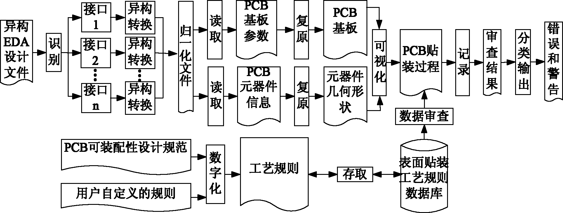
[0022] refer to figure 1 , the present invention examines the steps of printed circuit board electrical equipment data as follows:

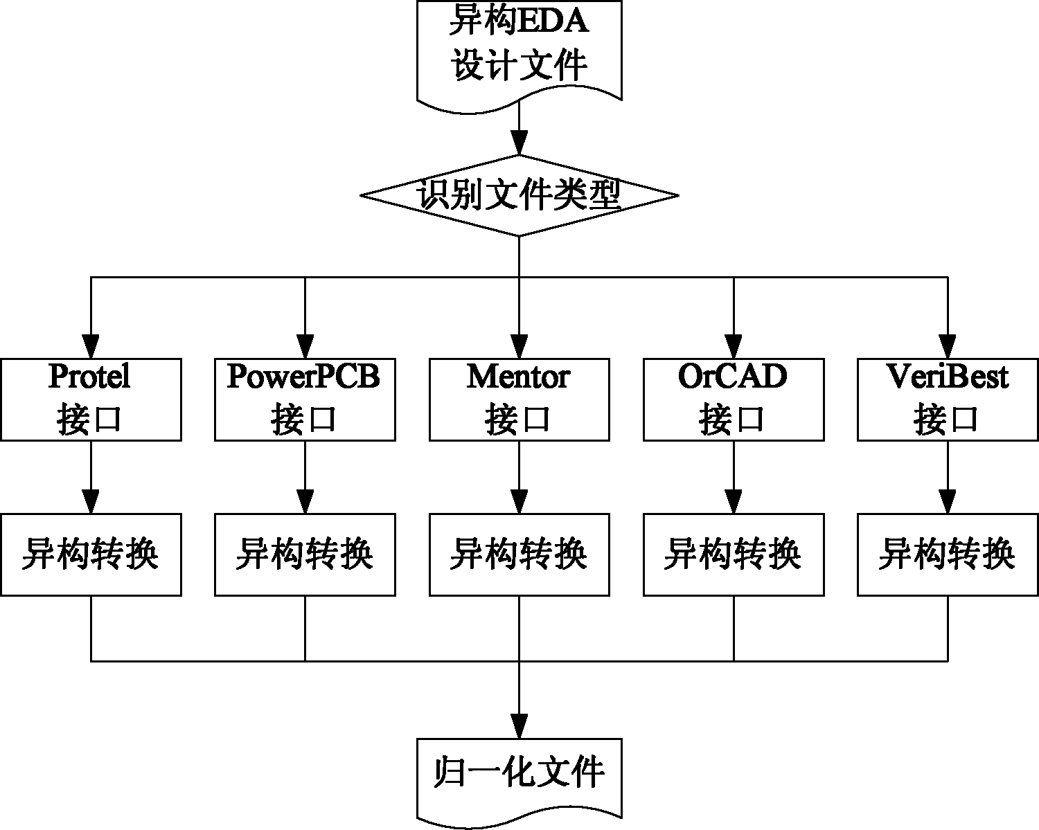
[0023] Step 1. Identify the types of heterogeneous EDA design files, send the files to different interfaces, extract and convert electrical equipment data, and generate normalized files.

[0024] refer to figure 2 , the specific implementation of this step is as follows:

[0025] (1a) Identify file types according to different EDA design file suffixes.

[0026] Among them, the heterogeneous EDA design file refers to the design file given by Protel, PowerPCB, Mentor, OrCAD and VeriBest software; the file suffix is ​​the suffix in the file name, that is, the suffix of the Protel file is .pcb, and the suffix of the PowerPCB file is . asc, the suffix of Mentor files is .mgc_component.attr, the suffix of OrCAD files is .min, and the suffix of VeriBest files is .prj.

[0027] (1b) Transfer different EDA design files to the corresponding interfaces...


PUM


Abstract

The invention discloses a method for checking electric fitting data of a printed circuit board, which mainly solves the problem that the electric fitting data of the printed circuit board cannot be automatically checked in the prior art. The method comprises the following steps of: converting automatic design files of electronic design of different structures into normalized files; digitalizing the assembled design specifications of the printed circuit board into process rules for checking, establishing a surface mounting process rule database and storing the process rules; recovering geometric shapes of a substrate and components of the printed circuit board by using visualization technology, and three-dimensionally and dynamically displaying the mounting process of the printed circuit board; checking the assembly properties of the components to be mounted by using the surface mounting process rule database as a drive, and recording the checking results; and classifying the checking results, and outputting the checking results in a figure or graph mode. By the method, the data for the automatic design files of the electronic design of different structures can be automatically checked, and the checking results can be intuitively displayed; moreover, the method can be used for surface mounting production preparation of the electric fitting industry.

Description

technical field [0001] The invention belongs to the technical field of computers, relates to a method for reviewing electrical equipment data of printed circuit boards, and can be used for pre-production preparation of surface mounting in the electrical equipment industry. Background technique [0002] In electronic design and manufacturing, the printed circuit board (PCB), as a subsystem of electronic products, plays the role of the core module unit. However, there are many types of electronic design automation EDA design software on the market at present, and the PCB design results are generally saved in the format of each EDA software company, and there is no unified data storage format. Although some EDA design software adopts the method of mutually supporting data formats, it cannot directly extract the information for assembly, which brings many difficulties to the assemblability review of various electronic design files. [0003] EDA design software generally has the...

Claims


Application Information

Patent Timeline
Patent Type & Authority Applications(China)
IPC IPC(8): G06F17/50
Inventor 来新泉黄战武毕明路姜建国沈振芳刘永生陈晓泽李锦
Owner XIDIAN UNIV
Why Eureka
Try Eureka