Method for automatic check of process data of printed circuit board

A printed circuit board and data processing technology, applied in the direction of electrical digital data processing, special data processing applications, instruments, etc., can solve problems such as low efficiency, difficulties, lack of communication bridges, etc., and achieve the effect of improving efficiency and fast processing

Inactive Publication Date: 2014-03-12
XIDIAN UNIV
View PDF1 Cites 0 Cited by
  • Summary
  • Abstract
  • Description
  • Claims
  • Application Information

AI Technical Summary

Problems solved by technology

However, the review of PCB processing data still adopts the traditional model, and there is a lack of effective communication bridge between increasingly high-end design technology and processing technology: PCB designers output manufacturing data, and processing manufacturers' computer-aided manufacturing, that is, CAM engineers, according to the company Manufacturing data review specifications or personal experience, manual inspection of PCB manufacturability
This brings many difficulties to the communication between electronic circuit design and manufacturing. Not only is the efficiency low, the processing cycle is long, and manual inspection may not be able to eliminate most errors, and product quality cannot be guaranteed.
PCB processing adopts the method of mass production. PCB processing includes the production of inner and outer layers, and copper plating is required. It involves the use of various heavy metals. The process is complicated, the process is numerous, the manufacturing cost is high, and the consumption is large. The design mass production required by the processing capacity will inevitably produce waste products, which not only increases new electronic pollution, but also causes huge economic losses
[0003] Although foreign software provides a certain review function of design and manufacturing data, these software are not only expensive, but also the configuration is too complicated, the practicability and interactivity have great defects, and it is not convenient for design and processing personnel to use
At the same time, this type of software has been monopolized by foreign countries for a long time, and domestic companies lack a certain degree of autonomy in purchasing and using it, and there may be unknown backdoors in the software, which is not conducive to product development and use

Method used


Image

  • Method for automatic check of process data of printed circuit board
  • Method for automatic check of process data of printed circuit board
  • Method for automatic check of process data of printed circuit board

Examples


Embodiment 2

[0082] PCB processing data automatic review method is the same as embodiment 1

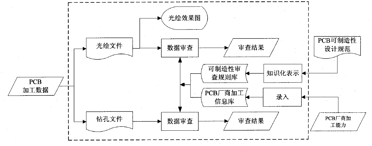
[0083] The inspection object of the present invention is the PCB manufacturing data file, which is a light drawing file and a drilling file that can be automatically exported by various electronic circuit design software, that is, a Gerber file and an NCDrill file. Gerber file is an international standard photo-painting format file, which includes RS-274-D and RS-274-X two formats, RS-274-D is called the basic Gerber format, and it must be accompanied by a D code file to Completely describe a graphic; RS-274-X is called the extended Gerber format, which itself contains D code information. Commonly used CAD software can generate files in both formats. The NCDrill file is a description of the drilling information in the same PCB design, and the format is the same as the Gerber file. For the two different formats RS-274-D and RS-274-X of the light painting file, the general data structure designed ...

Embodiment 3

[0086] The method for automatic inspection of PCB processing data is the same as in Embodiment 1-2

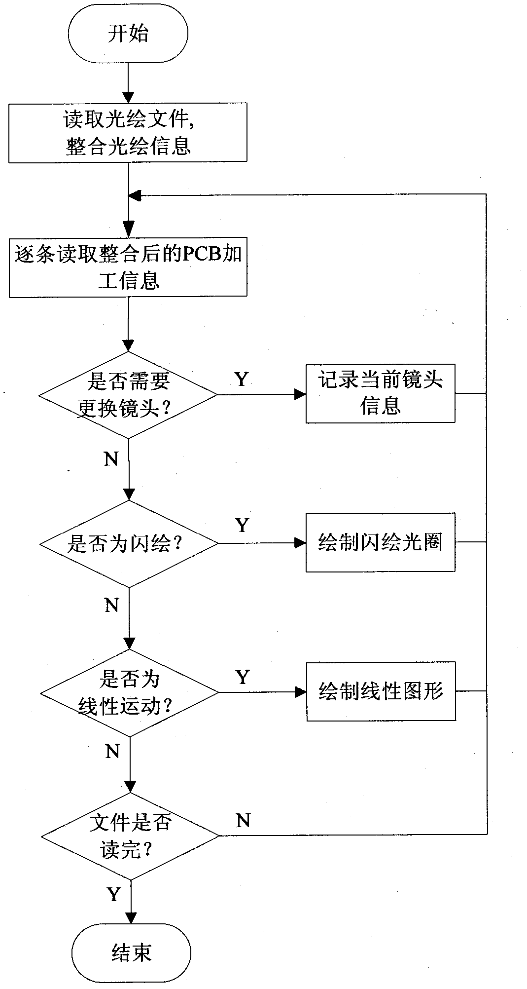
[0087] figure 2 It is a schematic diagram of the visualized flow chart of the PCB light-drawing file of the present invention. The invention can realize layered display of PCB light drawing files according to PCB design.

[0088] In the process of PCB light drawing, there are two main operation modes for the lens of the light plotter: linear motion and flash drawing. Among them, the linear movement in the PCB photopainting process is aimed at the wiring, silk screen and board frame in the PCB design, and the width of the line corresponds to the size of the aperture in the photopainting process. The invention can simulate the operation mode of the lens to draw the wiring in the PCB design , silk screen and board frame; and flash painting is aimed at the pads in PCB design. The diameter of the circular pad and the length and width of the rectangular pad correspond to the size ...

Embodiment 4

[0091] The method for automatic inspection of PCB processing data is the same as in Embodiment 1-3

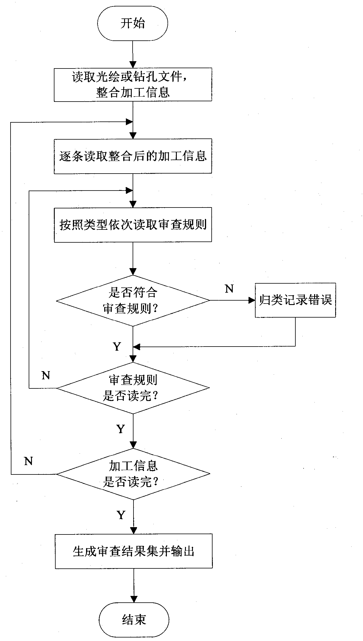
[0092] image 3 It is a schematic diagram of processing data review and result output flow in the present invention. The data review of drilling files is similar to that of gerber files, here we take the data review of gerber files as an example to illustrate.

[0093] The present invention firstly reads the light-painting file, and integrates the processing data in the file, reads the integrated light-painting processing information one by one, and then reads the rules in the review rule database according to the processing type of the currently read processing information, And review the processing data, if it does not meet the review rules, record this error, including error type, error location, error cause and other information, if it meets, continue to read the review rules until all the rules are read; after integration, each The processing information will cycle throu...


PUM


Abstract

The invention discloses a method for automatic check of process data of a printed circuit board (PCB), comprising formulating a manufacturability check rule according to a PCB manufacturability design specification; establishing a check rule database including the manufacturability check rule and PCB manufacturer processing information; reading PCB process data from light-plotting and drilling files introduced from an EDA; designing a universal data structure to integrate the process data; hierarchically and visually displaying a PCB light-plotting effect drawing; and calling the check rule during the check process to perform manufacturability check on the process data, performing a qualification check to the PCB manufacturer processing, and classifying and outputting the check result list. The method causes a user to be independent from an EDA (electronic design automation) design environment; the method is suitable for PCB manufacturers, professional EDA/CAD (computer aided design) companies and independent circuit design engineers to realize an automatic check function of PCB process data after finishing a PCB design and before processing and manufacturing; the method combines the processing capacities of the PCB manufacturers to perform manufacturability analysis, decrease the processing rejection rate and increase the production efficiency and product quality.

Description

technical field [0001] The invention belongs to the field of printed circuit board processing and manufacturing, mainly relates to electronic circuit design and manufacturing, and constructs an effective communication bridge between design and manufacturing, in particular to an automatic inspection method for PCB processing data. After the PCB design is completed and before the manufacturing process, the manufacturability review of the PCB design processing data and the processing capability review of the PCB manufacturer can be carried out. Background technique [0002] After half a century of development, the printed circuit board industry started from the research and trial production of single-sided, double-sided and metal perforated boards to the production of single-sided, double-sided, multi-layer and flexible boards. With the improvement of the design level, the enhancement of electronic design automation (EDA software function), the improvement of processing technol...

Claims


Application Information

Patent Timeline
Patent Type & Authority Patents(China)
IPC IPC(8): G06F17/50
Inventor 臧明相李社教来新泉王睿智甄立冬黄战武姜建国李斌宋英英
Owner XIDIAN UNIV
Why Eureka
Try Eureka