

Apparatus including an overlay mark and method of producing semiconductor assembly
A technology for alignment marks and semiconductors, applied in semiconductor devices, semiconductor/solid-state device manufacturing, electric solid-state devices, etc., can solve problems such as small geometric size, chip failure, and unsatisfactory aspects, and achieve alignment precision And the effect of accuracy and chip yield improvement
- Summary
- Abstract
- Description
- Claims
- Application Information
AI Technical Summary
Problems solved by technology
Method used
Image

Examples
Embodiment Construction
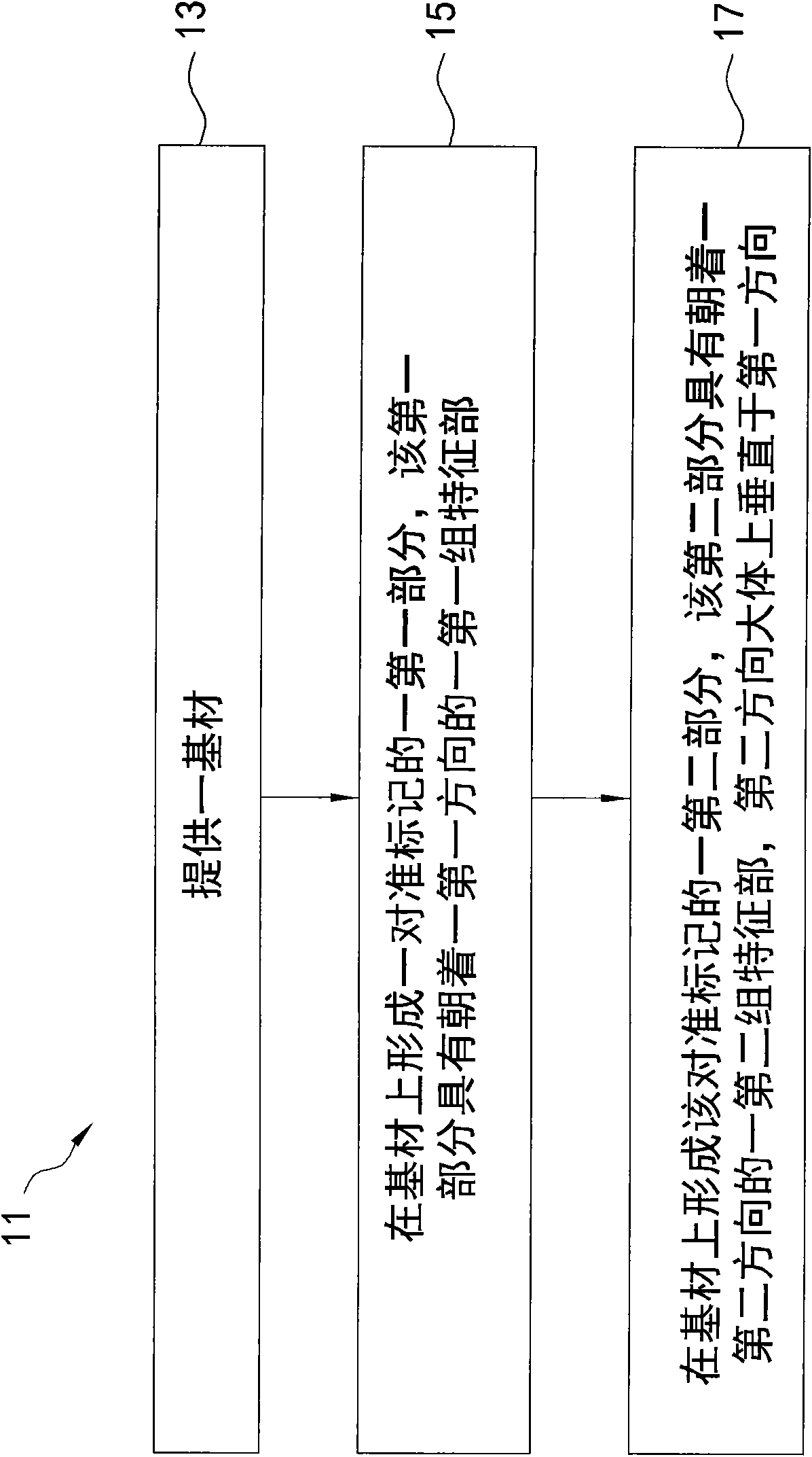
[0128] It should be understood that the present disclosure provides many different embodiments, or examples, by which various features of the invention can be implemented. Specific examples of components and arrangements are disclosed below to simplify the description of the present invention. Of course, these are just examples and are not intended to limit the present invention. In addition, forming the first feature on or over the second feature of the present invention may include various embodiments where the first and second features are formed in direct contact, and may include intercalating formation of the first and second features. Multiple embodiments of additional features between such that the first and second features are not in direct contact. Various features may be arbitrarily drawn in different scales for simplicity and clarity.
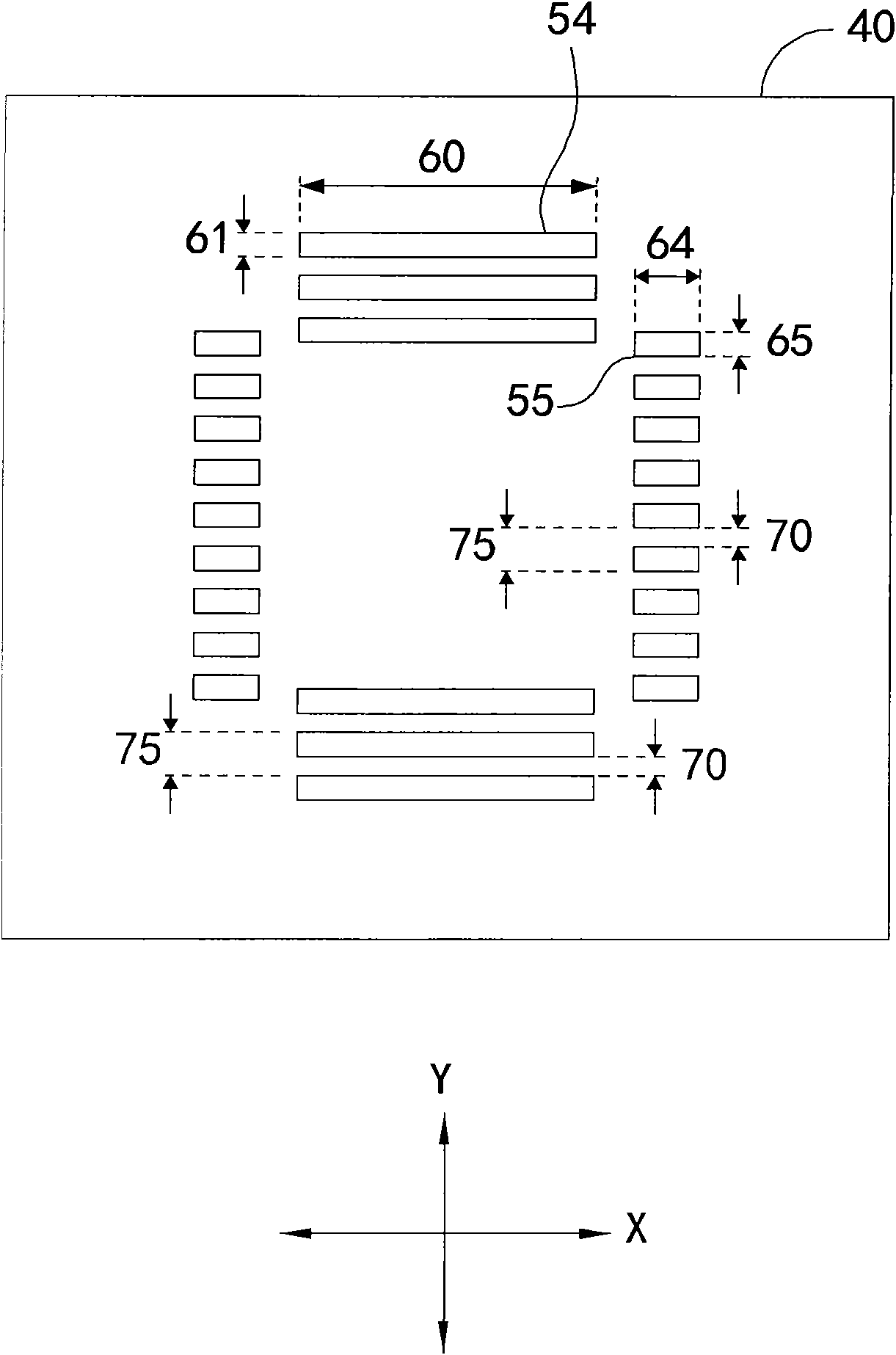
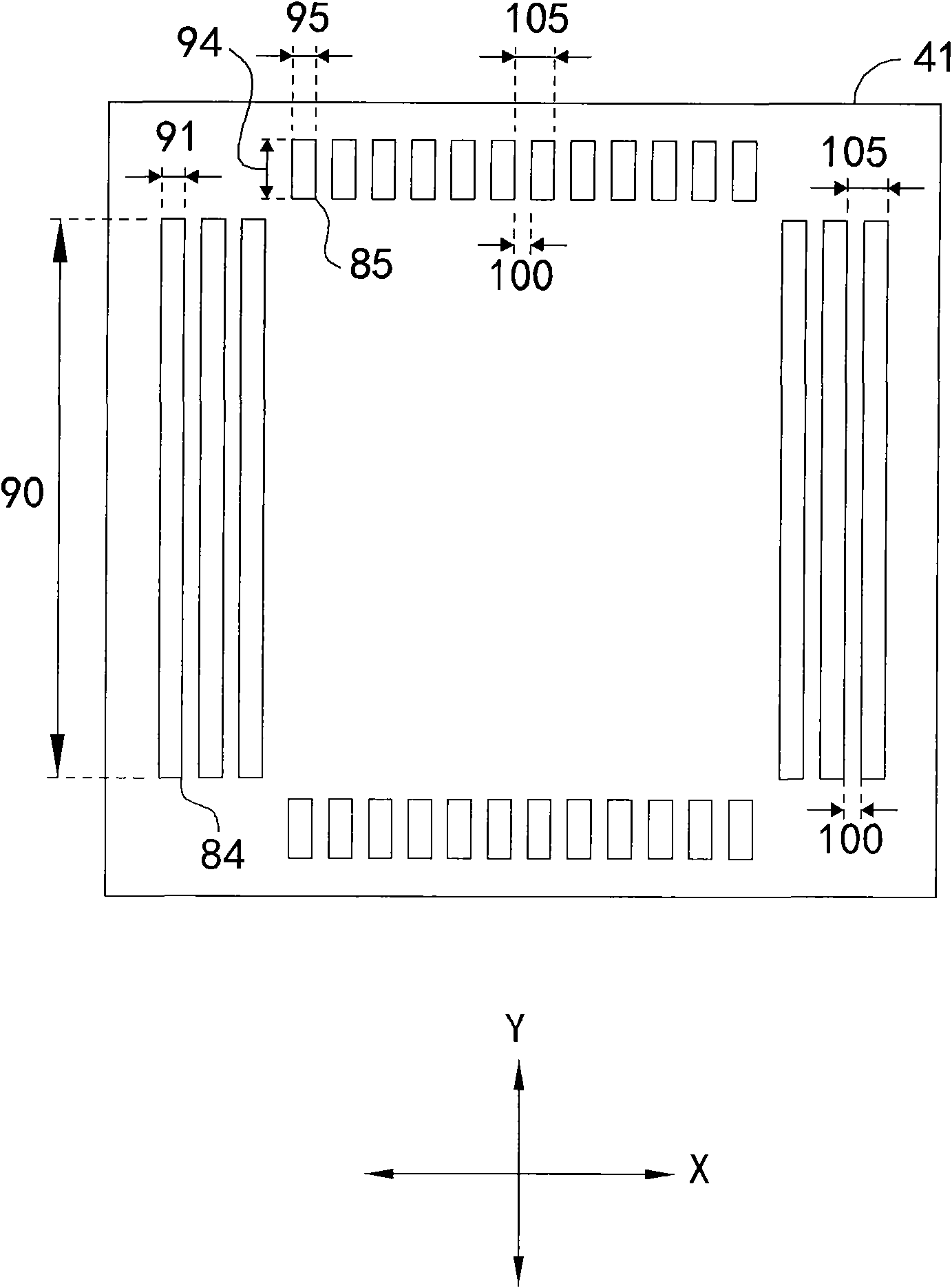
[0129] figure 1 Shown is a flowchart of a method for manufacturing alignment marks according to various aspects disclosed in the...
PUM
 Abstract
Description
Claims
Application Information