Electronic chip with dredging gap and substrate

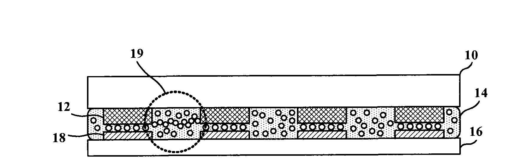
A technology for electronic chips and substrates, which is applied to circuits, electrical components, electrical solid devices, etc., can solve the problems of increasing the probability of conductive particles 14A being connected to each other, and difficult to flow smoothly.

Inactive Publication Date: 2011-07-06
RAYDIUM SEMICON
View PDF0 Cites 8 Cited by
  • Summary
  • Abstract
  • Description
  • Claims
  • Application Information

AI Technical Summary

Problems solved by technology

The inventors of the present invention have found that the conductive particles 14A flowing in the gaps are easily restricted by the right-angled corners around the...

Method used


Image

  • Electronic chip with dredging gap and substrate
  • Electronic chip with dredging gap and substrate
  • Electronic chip with dredging gap and substrate

Examples


Embodiment Construction

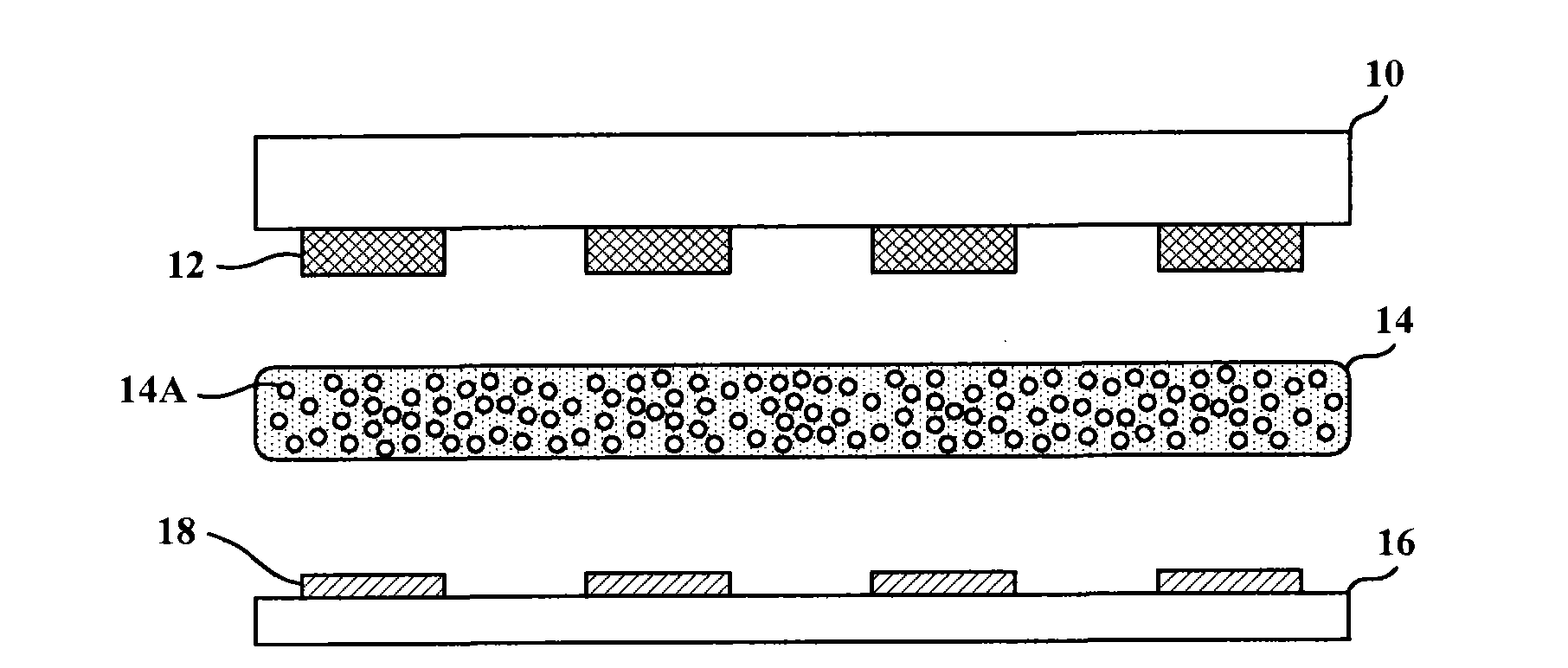
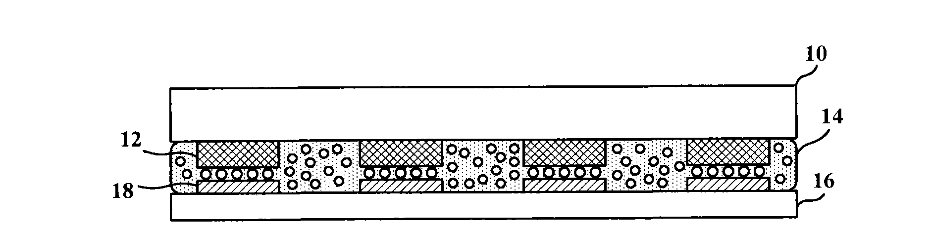
[0026] A first embodiment according to the present invention is an electronic chip including a plurality of conductive pins. The conductive pins are disposed on the outer surface of the electronic chip, and provide multiple electrical connections between the electronic chip and external circuits through conductive glue. Please refer to FIG. 2(A). FIG. 2(A) is a perspective view of the conductive pin 22 according to the present invention. In this example, the conductive pin 22 can be regarded as a polygonal column formed by truncating four corners of a rectangular column. As shown in FIG. 2(A), the cross section of the cylinder parallel to the outer surface of the electronic chip is approximately octagonal.

[0027] In practical application, the above-mentioned conductive adhesive for bonding the electronic chip and the external circuit may be anisotropic conductive adhesive (ACA), anisotropic conductive film (ACF), or Other types of jelly contain conductive particles.

[00...


PUM


Abstract

The invention provides an electronic chip which comprises a plurality of conductive pins, wherein the conductive pins are arranged on the external surface of the electronic chip and used for providing a plurality of electrical connections between the electronic chip and an external circuit through a conductive adhesive, the first conductive pin of the conductive pins is adjacent to the second conductive pin, and a first dredging gap is formed at a corner of the first conductive pin, which is adjacent to the second conductive pin, so as to provide a circulation space for at least one conductive particle of the conductive adhesive. The invention also provides a substrate. By adopting the electronic chip and the substrate provided by the invention, the probability of the occurrence of short circuit among the conductive pins can be effectively reduced.

Description

technical field [0001] The present invention relates to external conductive points of electronic chips / substrates, and more particularly to techniques for reducing the probability of short circuits between conductive points. Background technique [0002] With the development of science and technology in recent years, various commercial, household and personal electronic products are increasingly popular. In addition to enhancing functions and beautifying the appearance, the development trend of many electronic products also includes reducing the size of products to improve their portability and convenience in use. Due to the advancement of manufacturing technology and packaging technology, the area / volume of most electronic chips can indeed meet the above lightweight requirements. However, such a change also brings out many new problems and challenges for product designers or manufacturers. [0003] Please refer to Figure 1(A) to Figure 1(D). FIG. 1(A) to FIG. 1(D) are sc...

Claims


Application Information

Patent Timeline
IPC IPC(8): H01L23/482H01L23/488H01L23/12
CPCH01L2224/16225H01L2224/32225H01L2224/73204H01L2224/83101
Inventor 林青山吴世烽
Owner RAYDIUM SEMICON
Why Eureka
Try Eureka