Method for manufacturing nitride semiconductor device

A technology of nitride semiconductors and manufacturing methods, applied in semiconductor/solid-state device manufacturing, optical waveguide semiconductor structure, semiconductor devices, etc., can solve the problems of entering the active layer, deterioration of the active layer, deterioration of device characteristics, etc.

Inactive Publication Date: 2011-07-20
MITSUBISHI ELECTRIC CORP
View PDF8 Cites 9 Cited by
  • Summary
  • Abstract
  • Description
  • Claims
  • Application Information

AI Technical Summary

Problems solved by technology

In addition, InGaN having an In content exceeding 20% ​​tends to deteriorate due to heat, so there is a problem that the active layer deteriorates due to the growth process of the capping layer or contact layer grown on the InGaN active layer or the heat treatment in the wafer process process. , the luminous efficiency decreases, and the device characteristics deteriorate
[0008] However, using only hydrazine as the Group V source gas has the following problems: the high quality of the InGaN active layer is not sufficient, and especially in the case of emitting visible light from blue to green, the luminous characteristics deteriorate
In addition, there is a problem that even if the p-layer is grown at 900°C or lower, thermal damage enters the active layer during high-temperature annealing at 800°C to 1,000°C for activating Mg used as a p-type dopant, deteriorating the light-emitting characteristics

Method used


Image

  • Method for manufacturing nitride semiconductor device
  • Method for manufacturing nitride semiconductor device
  • Method for manufacturing nitride semiconductor device

Examples


Embodiment approach 1

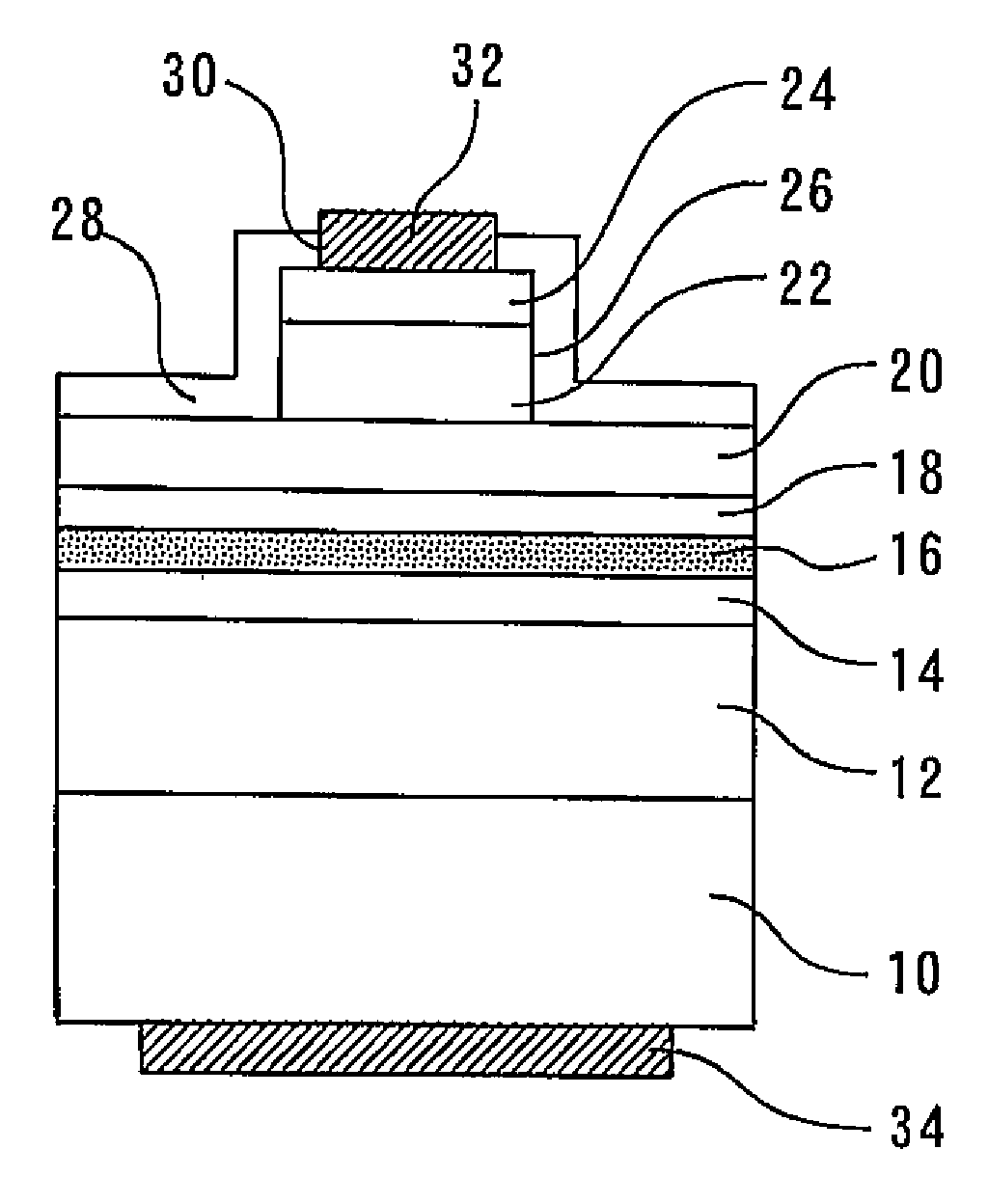
[0039] figure 1 It is a sectional view showing the nitride semiconductor device of Embodiment 1. This nitride semiconductor device is a nitride-based semiconductor laser.

[0040] On the (0001) plane which is the main surface of the n-type GaN substrate 10, n-type Al with a thickness of 2.0 μm is sequentially formed. 0.03 Ga 0.97 N cladding layer 12, n-type GaN optical guiding layer 14 with a thickness of 0.1 μm, active layer 16, p-type Al with a thickness of 0.02 μm 0.2 Ga 0.8 N electron blocking layer 18, p-type GaN optical guiding layer 20 with a thickness of 0.1 μm, and p-type Al with a thickness of 0.5 μm 0.03 Ga 0.97 An N cladding layer 22 and a p-type GaN contact layer 24 with a thickness of 0.06 μm.

[0041] p-type Al 0.03 Ga 0.97 The N cladding layer 22 and the p-type GaN contact layer 24 form a waveguide ridge 26 . The waveguide ridge 26 is formed at the center portion in the width direction of the resonator, and extends between two cleavage planes which bec...

Embodiment approach 2

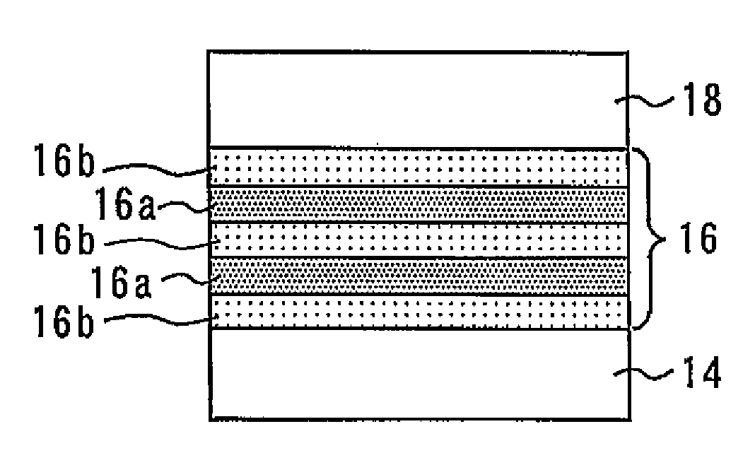
[0085] Figure 8 It is a sectional view showing the nitride semiconductor device of Embodiment 2. Figure 9 will be Figure 8 An enlarged cross-sectional view of the active layer of a nitride semiconductor device. The active layer 36 is used instead of the active layer 16 of the first embodiment. Other structures are the same as those in Embodiment 1.

[0086] The active layer 36 is Al with a thickness of 3.0 nm 0.01 In 0.21 Ga 0.78 N well layer 36a and Al with a thickness of 16.0nm 0.01 In 0.015 Ga 0.975 The N barrier layers 36b are alternately laminated with two pairs of multiple quantum well structures.

[0087] A method of manufacturing the active layer 36 will be described. First, while supplying NH 3 gas while changing the temperature of n-type GaN substrate 10 to 750°C. Then, as a carrier gas, in N 2 A small amount of H is mixed in the gas 2 Gas, feed ammonia, 1,2-dimethylhydrazine, TMG, TMI, TMA, form Al 0.01 In 0.21 Ga 0.78 N well layer 36a and Al 0....

Embodiment approach 3

[0090] Figure 10 It is a cross-sectional view showing a nitride semiconductor device according to Embodiment 3. Figure 11 will be Figure 10 An enlarged cross-sectional view of the active layer of a nitride semiconductor device. The active layer 38 is used instead of the active layer 16 of the first embodiment. Other structures are the same as those in Embodiment 1.

[0091] The active layer 38 is In with a thickness of 3.0 nm 0.2 Ga 0.8 N well layer 38a and Al with a thickness of 16.0nm 0.03 In 0.002 Ga 0.968 N barrier layers 38b are alternately laminated with two pairs of multiple quantum well structures.

[0092] A method of manufacturing the active layer 38 will be described. First, while supplying NH 3 gas while changing the temperature of n-type GaN substrate 10 to 750°C. Then, as a carrier gas, in N 2 A small amount of H is mixed in the gas 2 Gas, supply ammonia, 1,2-dimethylhydrazine, TMG, TMI, form In 0.2 Ga 0.8 N well layer 38a. Then, feed ammonia, ...


PUM

PropertyMeasurementUnit
thicknessaaaaaaaaaa
thicknessaaaaaaaaaa
thicknessaaaaaaaaaa

Abstract

The present invention relates to a method for manufacturing a nitride semiconductor device. A n-type Al0.03Ga0.97N covering layer (12) and a n-type GaN light guide layer (14) are formed on a n-type GaN substrate (10). On the n-type GaN light guide layer (14), ammonia and hydrazine derivative are used as group-V materials. Hydrogen is added in the carrier gas for forming an active layer (16) which is composed of the nitride semiconductor device which contains In. On the active layer (16), the ammonia and hydrazine derivative are used as group-V materials for forming a p-type AlO.2Ga0.8N electron barrier layer (18), a p-type GaN light guide layer (20), a p-type Al0.03Ga0.97N clad layer (22) and a p-type GaN contact layer (24).

Description

technical field [0001] The present invention relates to a method for manufacturing a nitride semiconductor device composed of a group III-V nitride-based semiconductor, and particularly to a method for manufacturing an excellent nitride semiconductor device with a simple process. Background technique [0002] Research and development of Group III-V nitride-based semiconductors are widely carried out as materials for light-emitting elements such as semiconductor laser elements and light-emitting diodes, or electronic devices. Taking advantage of its characteristics, blue light-emitting diodes, green light-emitting diodes, and blue-violet semiconductor lasers as light sources for high-density optical discs have been put into practical use. [0003] In the crystal growth of nitride-based semiconductors, ammonia (NH 3 )being widely used. In addition, since InGaN used in the active layer of a light-emitting element is easily re-evaporated from the surface, it does not crystalli...

Claims


Application Information

Patent Timeline
Patent Type & Authority Applications(China)
IPC IPC(8): H01S5/343
CPCH01S2304/04H01S5/3086H01L21/02458H01L21/02389H01S5/3201H01S5/22H01L21/0262H01S5/34333H01L21/02576H01L33/0075H01L21/02579B82Y20/00H01L21/0254
Inventor 大野彰仁竹见政义山本高裕
Owner MITSUBISHI ELECTRIC CORP
Why Eureka
Try Eureka