Ball grid array (BGA) substrate multilayer interconnection structure based on selective aluminum anodizing, and BGA substrate multilayer interconnection method based on selective aluminum anodizing

A multi-layer interconnection and anodized aluminum technology, which is applied in semiconductor/solid-state device components, semiconductor devices, electrical components, etc., can solve problems such as poor heat dissipation characteristics, large shrinkage rate, and limited use

Active Publication Date: 2014-11-19
SHANGHAI SPACEFLIGHT ELECTRONICS & COMM EQUIP RES INST
View PDF5 Cites 2 Cited by
  • Summary
  • Abstract
  • Description
  • Claims
  • Application Information

AI Technical Summary

Problems solved by technology

Although the sensitivity to moisture and the matching with the CTE of the chip have been solved, for high-power chip packaging and high-frequency device packaging, poor heat dissipation characteristics and large shrinkage are the main features, which limits its use in high-power and high-frequency device packaging. Especially in CBGA packaging, assembly problems of CBGA-FR4 substrates, CTE mismatch and elastic modulus difference, large stress on solder joints, and short thermal fatigue life

Method used


Image

  • Ball grid array (BGA) substrate multilayer interconnection structure based on selective aluminum anodizing, and BGA substrate multilayer interconnection method based on selective aluminum anodizing
  • Ball grid array (BGA) substrate multilayer interconnection structure based on selective aluminum anodizing, and BGA substrate multilayer interconnection method based on selective aluminum anodizing
  • Ball grid array (BGA) substrate multilayer interconnection structure based on selective aluminum anodizing, and BGA substrate multilayer interconnection method based on selective aluminum anodizing

Examples


Embodiment Construction

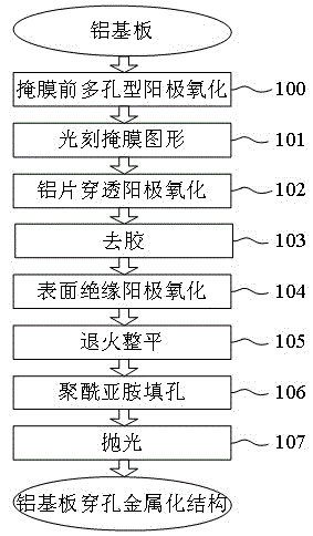
[0054] The technical solutions in the embodiments of the present invention will be clearly and completely described and discussed below in conjunction with the accompanying drawings of the present invention. Obviously, what is described here is only a part of the examples of the present invention, not all examples. Based on the present invention All other embodiments obtained by persons of ordinary skill in the art without creative efforts fall within the protection scope of the present invention.

[0055] In order to facilitate the understanding of the embodiments of the present invention, specific embodiments will be taken as examples for further explanation below in conjunction with the accompanying drawings, and each embodiment does not constitute a limitation to the embodiments of the present invention.

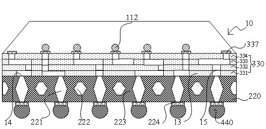
[0056] Such as figure 1 As shown, a BGA substrate multilayer interconnection structure 10 based on selective aluminum anodic oxidation provided by the present invention ...


PUM

PropertyMeasurementUnit
thicknessaaaaaaaaaa
thicknessaaaaaaaaaa
thicknessaaaaaaaaaa

Abstract

The present invention discloses a BGA substrate multilayer interconnection structure based on selective aluminum anodizing, and a BGA substrate multilayer interconnection method based on selective aluminum anodizing. According to the present invention, an upper-layer film multilayer interconnection structure and a lower-layer aluminum substrate perforating metallization structure are manufactured by a selective aluminum anodizing technology, a plurality of conduction bands in the tantalum-aluminum alloy films of the upper-layer film multilayer interconnection structure are electrically connected with a plurality of conduction bands of the aluminum films respectively, the plurality of conduction bands on the connection surfaces of the adjacent two sets of tantalum-aluminum alloy films and aluminum films are connected electrically and respectively, and the plurality of conduction bands in the tantalum-aluminum alloy films deposited on the lower-layer aluminum substrate perforating metallization structure are electrically connected with the upper ends of a plurality of aluminum flux columns respectively, thereby simplifying the manufacture process of a BGA substrate, reducing the cost of the BGA substrate, and improving the stability of the interconnection structure.

Description

technical field [0001] The invention relates to the technical field of semiconductor packaging, in particular to a BGA substrate multilayer interconnection structure and a manufacturing method based on a selective aluminum anodic oxidation process. Background technique [0002] BGA package, namely ball grid array package, is a new type of surface mount large-scale integrated circuit package. Compared with QFP (Quad Flat Package), it realizes the large-scale integrated circuit from four-side lead package to ball grid array package. The BGA package has the following notable features: BGA package provides a high number of I / O terminals, which is suitable for MCM package and realizes the high density of MCM; BGA package makes the signal path short, reduces parasitic inductance and capacitance, and improves electrical performance; BGA package The coplanar nature of the package and the "self-alignment" effect of the surface tension of the solder balls when they melt improve interc...

Claims


Application Information

Patent Timeline
Patent Type & Authority Applications(China)
IPC IPC(8): H01L23/538H01L21/768
CPCH01L2224/16225H01L2224/32145H01L2224/32225H01L2224/48091H01L2224/48227H01L2224/73204H01L2224/73265H01L2924/00014H01L2924/00
Inventor 王立春
Owner SHANGHAI SPACEFLIGHT ELECTRONICS & COMM EQUIP RES INST
Why Eureka
Try Eureka