Method for improving roughness of line edge of photoetching pattern in semiconductor process

A technology of edge roughness and photolithographic patterns, which is applied in the field of semiconductor manufacturing technology, can solve problems such as complex process, lower device yield, and increase production cost, and achieve the effect of simple process, improved line edge roughness, and low cost

Active Publication Date: 2013-04-10
SEMICON MFG INT (SHANGHAI) CORP +1
View PDF0 Cites 0 Cited by
  • Summary
  • Abstract
  • Description
  • Claims
  • Application Information

AI Technical Summary

Problems solved by technology

[0009] This improved method of using amorphous carbon as a hard mask to form a pattern according to the traditional process can improve the LER of the pattern to a certain extent, but it has the disadvantage of complex process
In addition, amorphous carbon is expensive, which greatly increases the production cost
Secondly, due to the porosity and loose texture of the amorphous carbon material, it is extremely vulnerable to damage during the photolithography stage, which will lead to inaccurate transfer of the pattern and reduce the yield of the device.

Method used


Image

  • Method for improving roughness of line edge of photoetching pattern in semiconductor process
  • Method for improving roughness of line edge of photoetching pattern in semiconductor process
  • Method for improving roughness of line edge of photoetching pattern in semiconductor process

Examples


Embodiment Construction

[0029] In the following description, numerous specific details are given in order to provide a more thorough understanding of the present invention. It will be apparent, however, to one skilled in the art that the present invention may be practiced without one or more of these details. In other examples, some technical features known in the art are not described in order to avoid confusion with the present invention.

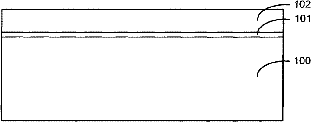
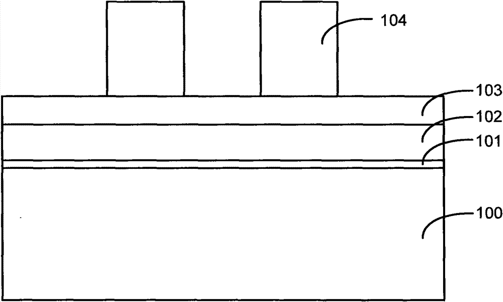
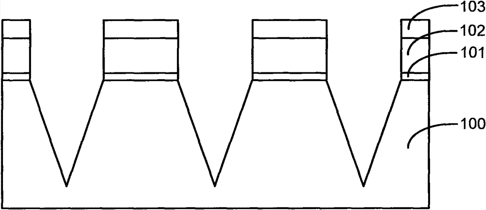
[0030] In order to thoroughly understand the present invention, detailed steps will be presented in the following description to illustrate how the present invention utilizes the photoresist stabilization injection process to improve the line edge roughness of the pattern. Obviously, the practice of the invention is not limited to specific details familiar to those skilled in the semiconductor arts. Preferred embodiments of the present invention are described in detail below, however, the present invention may have other embodiments besides these detailed descr...


PUM

PropertyMeasurementUnit
thicknessaaaaaaaaaa

Abstract

The invention provides a method for improving the roughness of the line edge of a photoetching pattern in a semiconductor process, which comprises the following steps of: coating photoresist on a semiconductor layer on which the pattern is needed to be formed; exposing and developing the photoresist to form the photoresist with the pattern; performing ion implantation on the photoresist with the pattern to form a hard mask; and etching the semiconductor layer by taking the hard mask as a mask. By the method, the roughness of the line edge of the pattern can be improved obviously; and the method has a simple process and is low in cost.

Description

technical field [0001] The invention relates to a semiconductor manufacturing process, in particular to a process for improving line edge roughness by means of ion implantation. Background technique [0002] As the size of integrated circuits (ICs) continues to decrease, the design rules of semiconductor devices have shrunk from 65nm to 45nm, and are currently developing towards 32nm or even smaller technology. The photolithography process is one of the most important steps in the process of scaling down the process size. However, the effect on the line edge roughness (LER) of the pattern caused by the photoresist (photoresist layer) exposure process is becoming more and more obvious, even unacceptable in the process below the 65nm node. Therefore, it is necessary to improve the LER of the pattern by increasing the requirements on the equipment. [0003] In Calvin Gabriel's article published at the ICMI conference in 2003, the industry standard for measuring the unevenness...

Claims


Application Information

Patent Timeline
Patent Type & Authority Patents(China)
IPC IPC(8): H01L21/027G03F7/00
Inventor 李亮沈忆华涂火金宋化龙史运泽
Owner SEMICON MFG INT (SHANGHAI) CORP
Why Eureka
Try Eureka