Single-layer projected capacitive touch panel and manufacturing method thereof
A technology of projected capacitance and touch panel, which is applied in the direction of electrical digital data processing, instrumentation, input/output process of data processing, etc., and can solve the problems of low light transmittance and production yield
- Summary
- Abstract
- Description
- Claims
- Application Information
AI Technical Summary
Problems solved by technology
Method used
Image

Examples
Embodiment Construction
[0060] see Figure 1A to Figure 1H As shown, a preferred embodiment of the single-layer projected capacitive touch panel of the present invention is manufactured by the following steps:
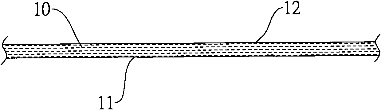
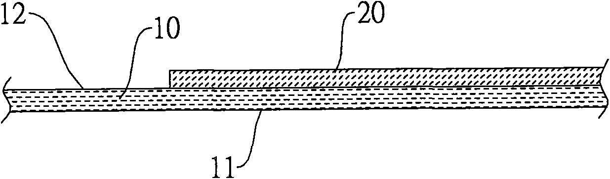
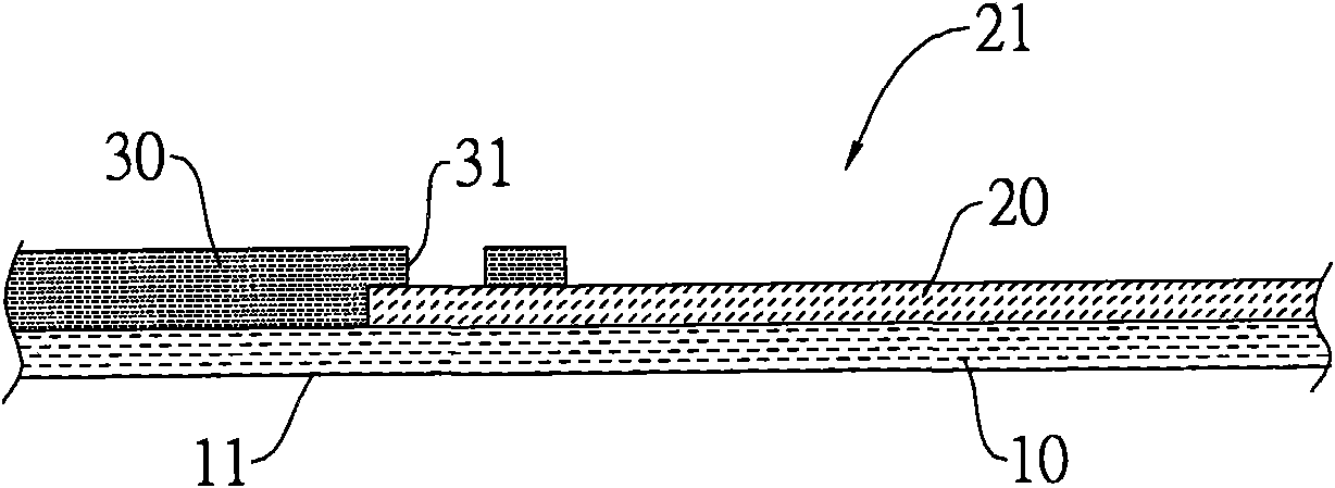
[0061] Prepare a mother glass plate, which can be divided into a plurality of glass cover plates 10 of the single-layer projected capacitive touch panel of the present invention (eg Figure 1A and figure 2 As shown), each glass cover plate 10 has an action surface 11 and a circuit surface 12;
[0062] Form a touch sensing circuit layer 20, such as Figure 1B As shown, a corresponding touch sensing circuit layer 20 is partially formed on the circuit surface 12 of each glass cover plate 10 of the glass mother board, as shown in FIG. figure 2 Shown is the central area of the circuit surface 12 of each glass cover plate 10, and each touch sensing circuit layer 20 is a single-layer touch sensing circuit, such as a single-layer indium tin oxide (Indium tinoxide, ITO for short) circuit compo...
PUM
 Abstract
Description
Claims
Application Information
 - R&D Engineer
- R&D Manager
- IP Professional
- Industry Leading Data Capabilities
- Powerful AI technology
- Patent DNA Extraction
Browse by: Latest US Patents, China's latest patents, Technical Efficacy Thesaurus, Application Domain, Technology Topic.
© 2024 PatSnap. All rights reserved.Legal|Privacy policy|Modern Slavery Act Transparency Statement|Sitemap