

Verifying environment patterned chip verifying method and device
A technology of verification environment and verification method, which is applied in the field of chip verification method and device with graphic verification environment, can solve the problem of no systematic operation of test case management and maintenance, complex and cumbersome chip function verification, unfavorable test case regression test and other issues to achieve the effect of shortening the chip verification cycle, reducing learning costs, and reducing learning costs
- Summary
- Abstract
- Description
- Claims
- Application Information
AI Technical Summary
Problems solved by technology
Method used
Image

Examples
Embodiment Construction
[0024] The present invention will be further described in detail below in conjunction with the accompanying drawings and embodiments.
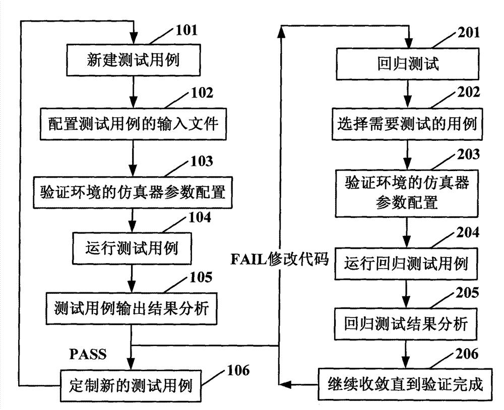
[0025] see figure 1 As shown, in the embodiment of the present invention, the chip verification method with a graphical verification environment has two branches in its basic process: one is for a single test case, and the other is for regression testing, that is, after an error case is found, the verification of the old code is completed Modification requires retesting multiple or all test cases to confirm that the modification does not introduce new errors or cause errors in other codes. The two branches are interleaved with each other. When testing a single use case error, it is necessary to perform a regression test after modifying the code.
[0026] The implementation process of a single test case is as follows:
[0027] Step 101: Create a new test case and group it according to functional test points and functional modules.
[0028] S...
PUM
 Abstract
Description
Claims
Application Information