

Method for eliminating redeposition of side wall of grid and semiconductor device
A gate sidewall and redeposition technology, applied in semiconductor/solid-state device manufacturing, transistors, electrical components, etc., can solve problems such as reducing circuit performance and device reliability, and achieve the effect of eliminating metal redeposition
- Summary
- Abstract
- Description
- Claims
- Application Information
AI Technical Summary
Problems solved by technology
Method used
Image

Examples
Embodiment Construction
[0022] In order to make the content of the present invention clearer and easier to understand, the content of the present invention will be described in detail below in conjunction with specific embodiments and accompanying drawings.
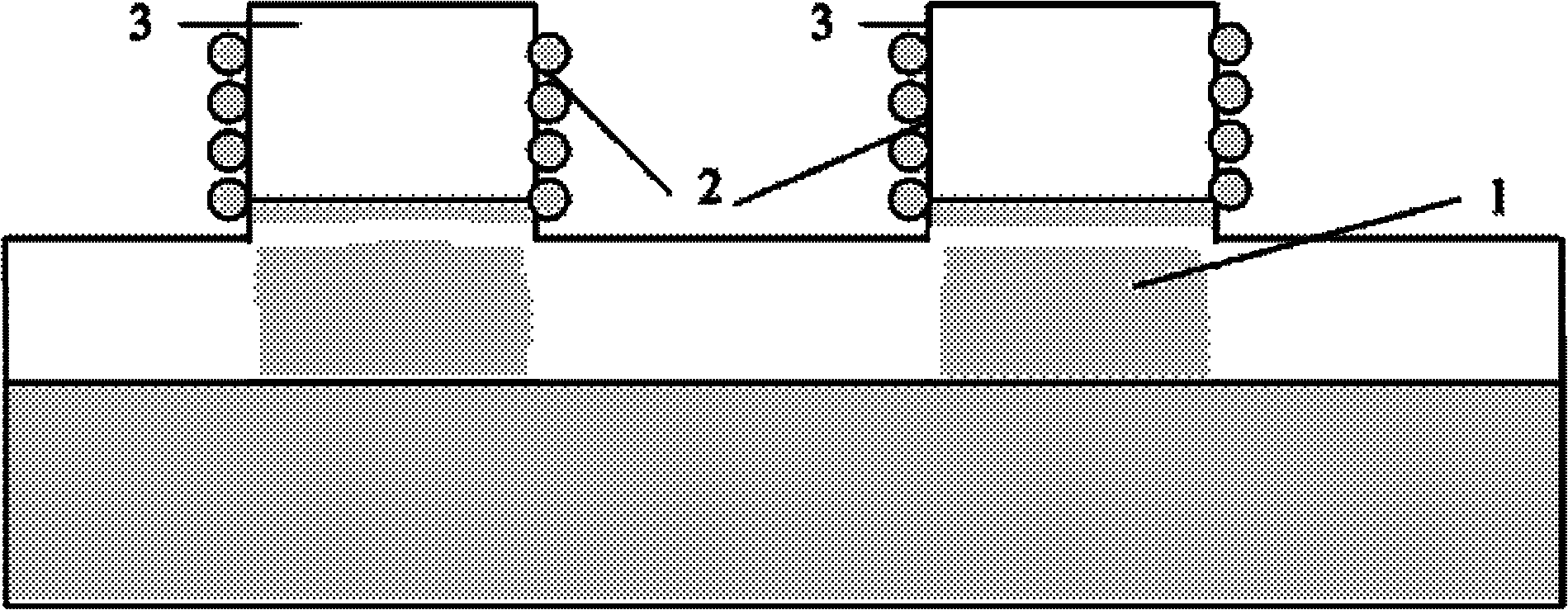
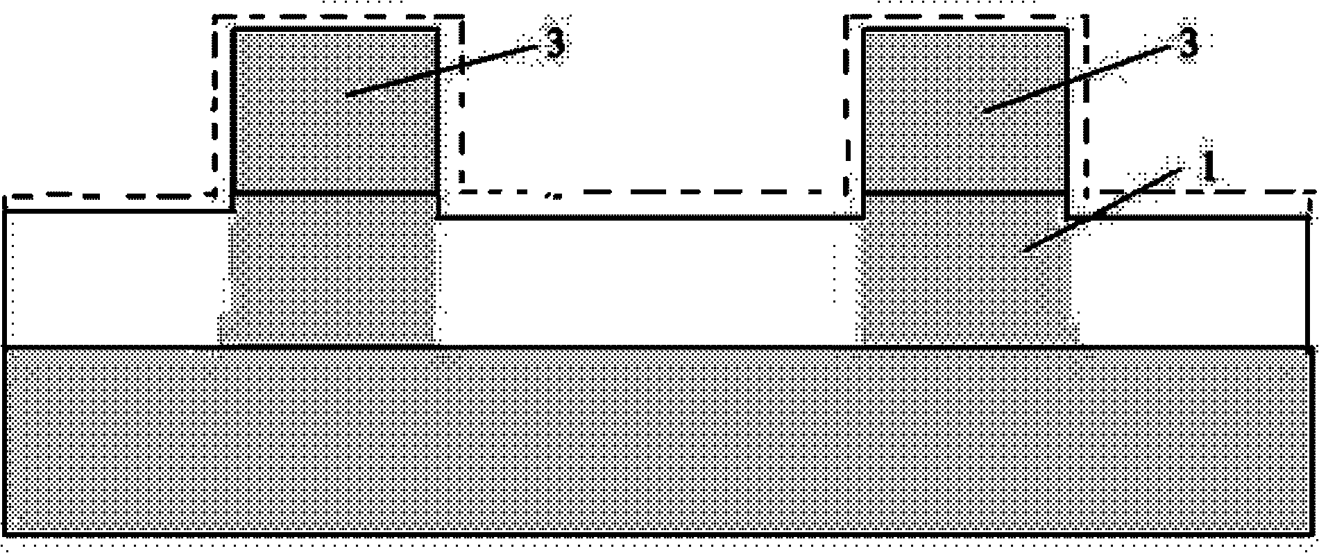
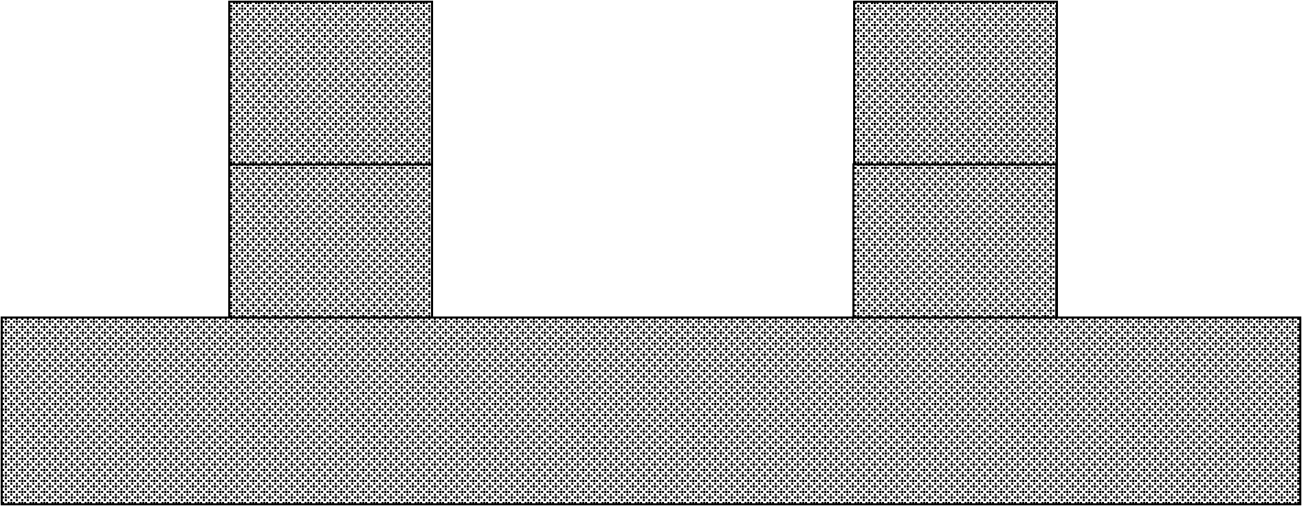
[0023] The method for eliminating gate sidewall redeposition according to an embodiment of the present invention includes: a gate sidewall impurity etching step, which is used to remove gate sidewall impurities during the etching process by adjusting the size of the hard mask.
[0024] Specifically, for example, a physical vapor deposition step of the gate may be used to deposit the gate material in the early stage. However, the present invention is not limited to the deposition method of the gate material, that is, the physical vapor deposition step does not limit the present invention in any form. Also, the physical vapor deposition step of the gate can be performed in any suitable manner.
[0025] In fact, the present invention is characteri...
PUM
 Abstract
Description
Claims
Application Information