
Resetting circuit

A technology for resetting circuits and pathways, applied to instruments, static indicators, etc., can solve problems such as wrong charging of pixel data in the screen, abnormal display of the screen, etc.

Inactive Publication Date: 2011-09-14
AU OPTRONICS CORP
View PDF8 Cites 12 Cited by
  • Summary
  • Abstract
  • Description
  • Claims
  • Application Information

AI Technical Summary

Problems solved by technology

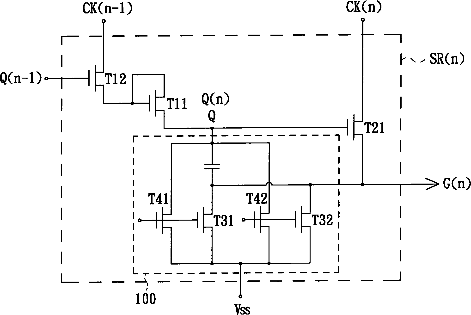
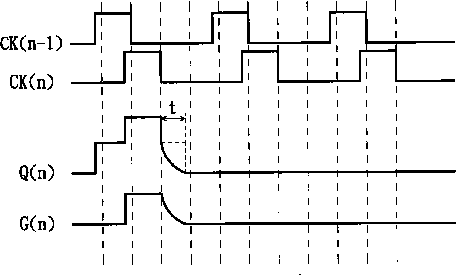
[0005] However, when the process variation of the transistors T41 and T42 in the pull-down circuit 100 is too large, it will cause the control signal Q(n) to leak to the gate-off signal level VSS earlier in the period t instead of as figure 2 As shown by the dotted line in the period t, the gate drive pulse G(n) cannot be closed normally, which will cause the gate drive pulse G(n) to drag (such as figure 2 The waveform of G(n) in the middle period t), when the dragging is too long, it will lead to wrong filling of pixel data in the screen, resulting in abnormal screen display

Method used


Image

  • Resetting circuit
  • Resetting circuit
  • Resetting circuit

Examples


Embodiment Construction

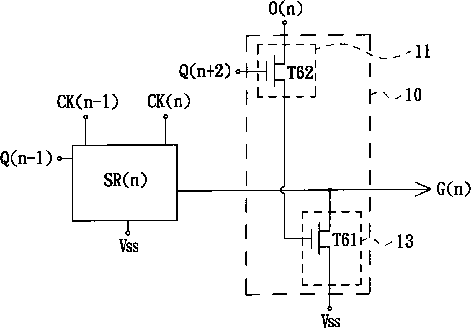
[0044] see Figure 3A , which is a schematic structural diagram of the reset circuit proposed in the first embodiment of the present invention. like Figure 3A As shown, the reset circuit 10 is electrically coupled to the output terminal of the shift register SR(n) (for outputting the gate driving pulse G(n)), and is used to adjust the output of the shift register SR(n) terminal potential; Figure 3A The shift register SR(n) in can be compared with figure 1 The shift register SR(n) in has the same circuit structure, but the present invention is not limited thereto; in addition, it should be noted that, Figure 3A The drawing of the reset circuit 10 outside the shift register SR(n) is only for distinguishing the difference between the present invention and the prior art, and is not used to limit whether the shift register SR(n) includes the reset circuit 10 .

[0045] Based on the above, this embodiment uses a single odd-numbered shift register SR(n) among multiple shift re...


PUM


Abstract

The invention discloses a resetting circuit for adjusting the potential of the output terminal of a shift buffer, which comprises a driving module and a resetting module of the resetting circuit. The driving module receives inducing signals and provides the inducing signals to the output terminal of the driving module. The resetting module is electrically coupled to the output terminal of the shift buffer and the output terminal of the driving module. The potential of the output terminal of the driving module controls whether the electricity between the output terminal of the shift buffer and a first preset potential is turned on or not by the resetting module.

Description

technical field [0001] The present invention relates to the field of display technology, and in particular to a structure of a reset circuit suitable for adjusting the potential of an output end of a shift register. Background technique [0002] Press, with the development of science and technology, flat panel displays (such as liquid crystal displays) are widely used in mobile phones, notebook computers, desktops, etc. due to their advantages of high image quality, small size, light weight and wide application range. In various consumer electronic products such as display devices and televisions, it has gradually replaced traditional cathode ray tube displays and become the mainstream of displays. [0003] At present, in order to reduce the cost of flat panel displays, Gate-on-Array (GOA) and Half-source Driving (HSD) technologies have been developed. Usually, the gate driving circuit on the array includes a plurality of shift registers connected in series to output a plur...

Claims


Application Information

Patent Timeline
IPC IPC(8): G09G3/20
Inventor 郑晓钟黄正翰
Owner AU OPTRONICS CORP
Learn More