
Thin mobile communication device

A mobile communication device and a technology for mobile communication, applied in the field of thin mobile communication devices, can solve the problems of the influence of the internal space configuration of the mobile communication device, the influence of the internal space configuration, the large and no ground plane interval, etc., and achieve good input impedance matching and radiation. Effects of Features

Active Publication Date: 2011-09-21
ACER INC
View PDF6 Cites 7 Cited by
  • Summary
  • Abstract
  • Description
  • Claims
  • Application Information

AI Technical Summary

Problems solved by technology

[0003] However, for the antenna designed in the above method, one side, especially the side including the end of the antenna or near the end, needs to have a clear space with the adjacent ground plane to reduce the influence on the radiation characteristics of the antenna. The required interval without a ground plane becomes larger, which reduces the integration degree of the antenna inside the mobile communication device and affects the configuration of the entire internal space.
[0004] For example, U.S. Patent Application Publication No. US2009 / 0273521 A1 "Coplanar Coupled-fed multiband antenna for the mobile device (coplanar coupled-fed multiband antenna for the mobile device)", which discloses a planar antenna suitable for wireless wide area network mobile communication work, The antenna is located in a non-ground plane area, but the non-ground plane area is only separated from the adjacent system ground plane by one edge, and cannot be closely combined with the system ground plane (at least two edges of the non-ground plane area are adjacent system ground planes. Surrounded by the ground plane), although the antenna can work in broadband, it still needs a large interval without a ground plane, which affects the configuration of the internal space of the entire mobile communication device

Method used


Image

  • Thin mobile communication device
  • Thin mobile communication device
  • Thin mobile communication device

Examples


Embodiment Construction

[0025] In order to make the above and other objects, features and advantages of the present invention more comprehensible, specific embodiments of the present invention are listed below and described in detail in conjunction with the accompanying drawings.

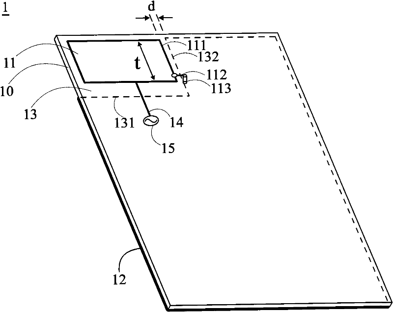
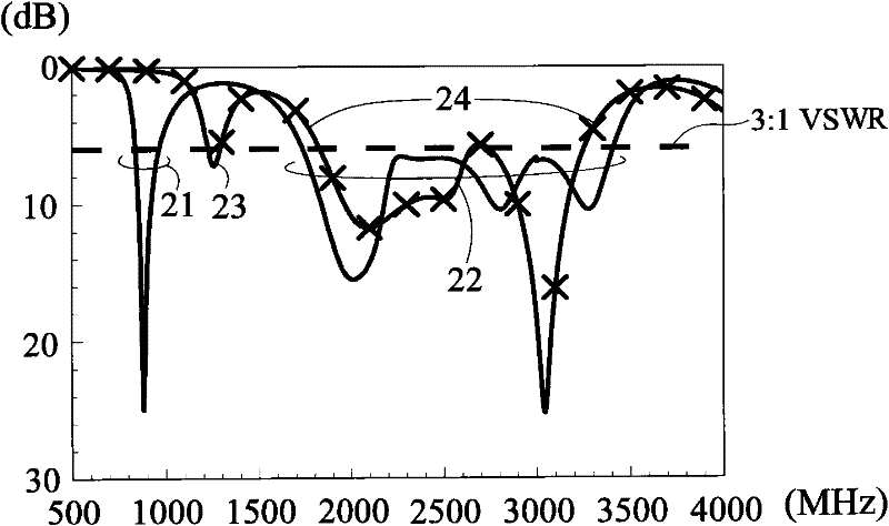
[0026] figure 1 It is a structural diagram of the first embodiment of the thin mobile communication device of the present invention. The thin mobile communication device 1 has a dielectric substrate 10 , a ground plane 12 and an antenna 11 . The dielectric substrate 10 can be a system circuit board of a mobile communication mobile phone, and the antenna 11 can be formed on the dielectric substrate 10 by printing or etching technology, and the antenna 11 is a planar structure, and the antenna 11 has a first working frequency band 21 and a second working frequency band 22 (eg figure 2 shown).

[0027] The antenna 11 is formed on the dielectric substrate 10 in the area 13 without a ground plane, and the area 13 without a ...


PUM


Abstract

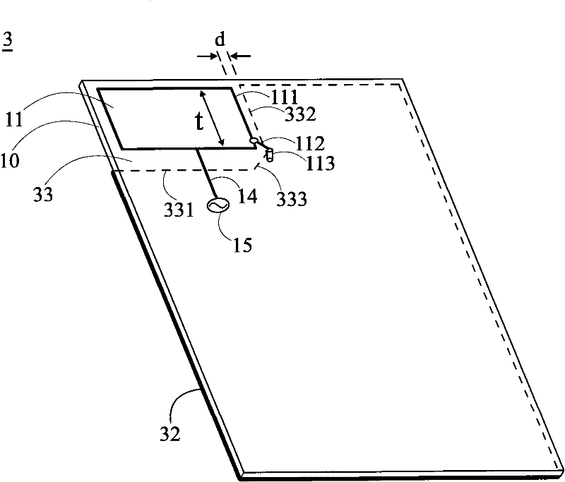
The invention discloses a thin mobile communication device. The thin mobile communication device comprises a medium substrate, a ground plane and an antenna, wherein the medium substrate comprises a ground plane-free interval comprising a first edge and a second edge; the ground plane is positioned on the medium substrate; the antenna, which is a planar structure, includes a first working frequency band and a second working frequency band and is formed in the ground plane-free interval on the medium substrate, the first edge and the second edge of the ground plane-free interval are surrounded by the ground plane, the first edge is used for the passage of a feed-in connecting wire of the antenna, the first edge is a feed-in edge and the second edge is a non-feed-in edge, the distance between a side of the antenna and the second edge is less than 3mm, and the side is at least 5mm long and is in short-circuit connection with the ground plane. The device of the invention can obtain excellent input impedance matching and radiation characteristics by tightly combining the antenna with the adjacent ground plane.

Description

technical field [0001] The invention relates to a thin mobile communication device, especially a thin mobile communication device whose built-in wireless wide area network (WWAN, Wireless Wide Area Network) antenna is closely combined with the adjacent system ground plane. Background technique [0002] In recent years, mobile communication devices have developed rapidly. Not only must their built-in antennas meet the requirements of wireless wide-area network work in the working frequency band (including at least two frequency bands of 824-960MHz and 1710-2170MHz), but also require their built-in antennas to be connected to the system ground plane. It can have high integration, so as to achieve the effective use of the internal space of the mobile communication device. Therefore, the design of the built-in antenna of the mobile communication device is not only light, thin, short, and small, but must also be tightly integrated with the ground plane of the adjacent system or w...

Claims


Application Information

Patent Timeline
IPC IPC(8): H01Q1/24H01Q1/38H01Q5/00H01Q5/10
Inventor 翁金辂陈威宇
Owner ACER INC
Learn More