

Stack structure for enhancing bonding strength of touch panel
A touch panel and touch technology, applied in the field of stack structure, to achieve the effect of sufficient bonding strength
- Summary
- Abstract
- Description
- Claims
- Application Information
AI Technical Summary
Problems solved by technology
Method used
Image

Examples
Embodiment Construction
[0032] The description of the present invention and other technical content, features and effects will be clearly presented in the following detailed description in conjunction with the embodiments in the accompanying drawings.
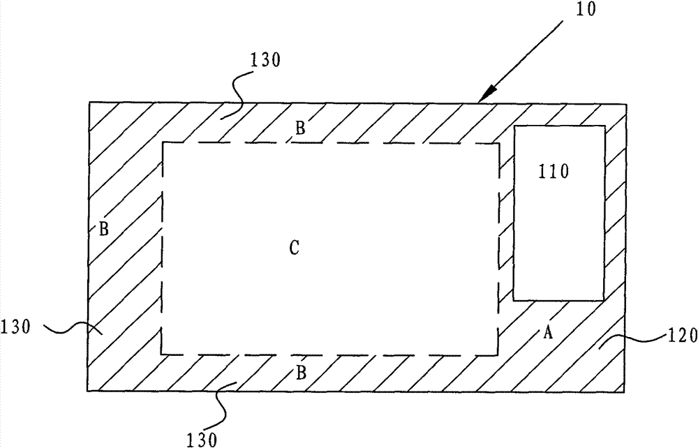
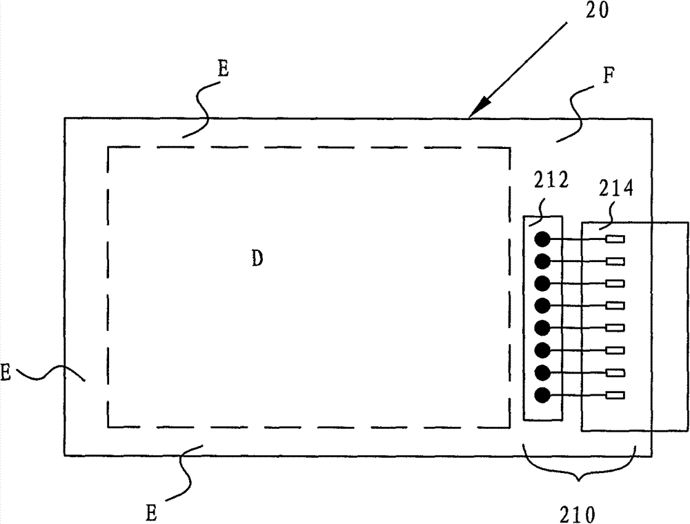
[0033] figure 1 and figure 2 Respectively show a part of the stacked structure of the first embodiment of the present invention to enhance the bonding strength of the touch panel, in which figure 1 is the top view of the mirror substrate 10 in the display stack structure, and figure 2 It is a top view of the touch substrate 20 in the stack structure.
[0034] Since some components need to be arranged on the mirror substrate 10 and the touch substrate 20 respectively to achieve the functions of touch control and beautiful appearance, the touch substrate 20 included in the stack structure of this embodiment has a bonding area F, An electrical component 210 is disposed between the bonding areas F. The electrical component 210 includes a conductive...
PUM
 Abstract
Description
Claims
Application Information