Substrate processing device

A substrate processing device and a technology for processing space, applied in the direction of electrical components, semiconductor/solid-state device manufacturing, circuits, etc., can solve the problem of increasing manufacturing costs, maintenance costs and repair costs, limiting the implementation of temperature control methods, and increasing the overall manufacturing of chambers cost and other issues, to achieve the effect of saving manufacturing cost and maintenance/repair cost, saving manufacturing cost, and minimizing thermal deformation

Inactive Publication Date: 2015-04-08
WONIK IPS CO LTD
View PDF6 Cites 0 Cited by
  • Summary
  • Abstract
  • Description
  • Claims
  • Application Information

AI Technical Summary

Problems solved by technology

This may increase the overall manufacturing cost, maintenance cost and repair cost, and may limit the implementation of temperature control methods
[0009] Third, it may not be easy to form a flow path in the wall of the chamber where the flow path is specially processed in the wall of the chamber
and this may increase the overall manufacturing cost of the chamber
[0010] Fourth, in the case where a heater for controlling the temperature of the processing space is installed on the outer wall surface of the chamber, the temperature control of the processing space may be affected by factors such as the chamber material, the external environment of the chamber, etc.
This may increase the overall temperature control volume

Method used


Image

  • Substrate processing device
  • Substrate processing device
  • Substrate processing device

Examples


Embodiment Construction

[0035] The present invention is described in detail with reference to the accompanying drawings.

[0036] Next, the substrate processing apparatus according to the present invention will be further described in detail with reference to the accompanying drawings.

[0037] A substrate processing apparatus according to the present invention is used to perform a predetermined process on a substrate. The substrate processing device may include all of a load lock device, a vacuum processing device, a transfer module, etc., or may include at least one of them.

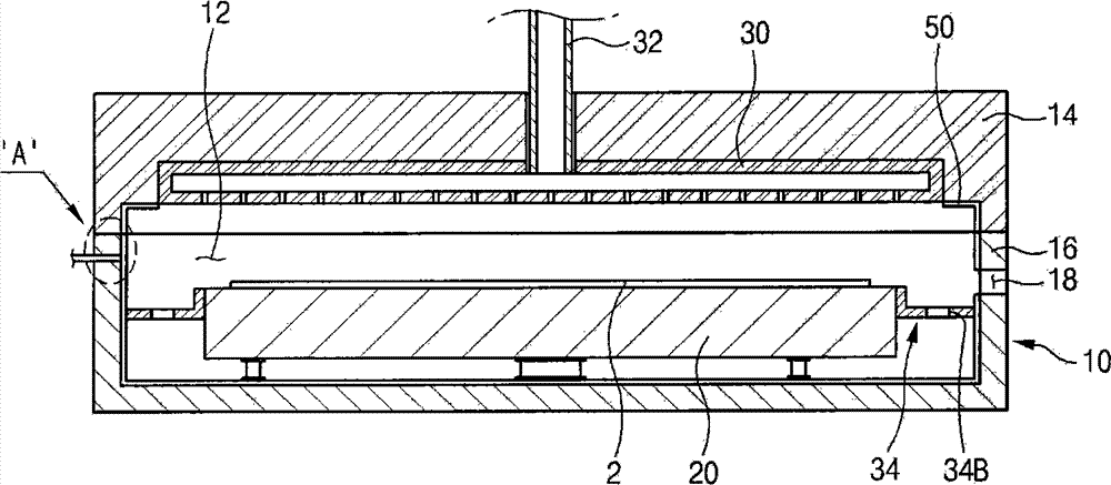
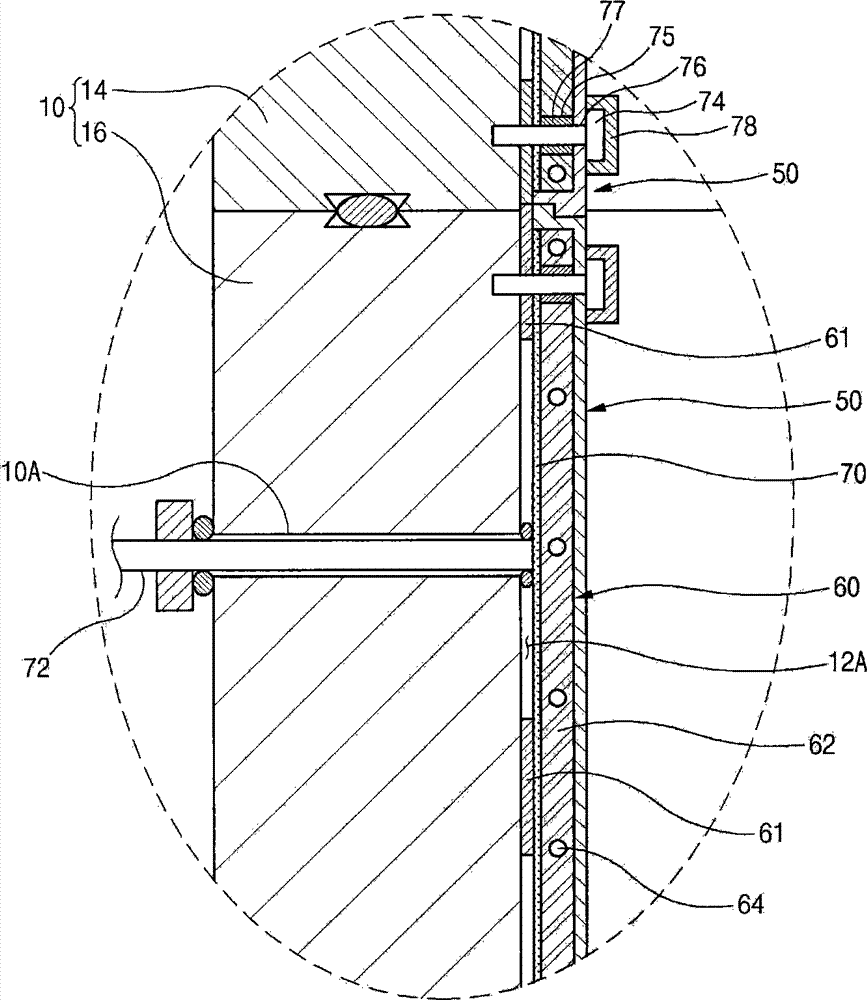
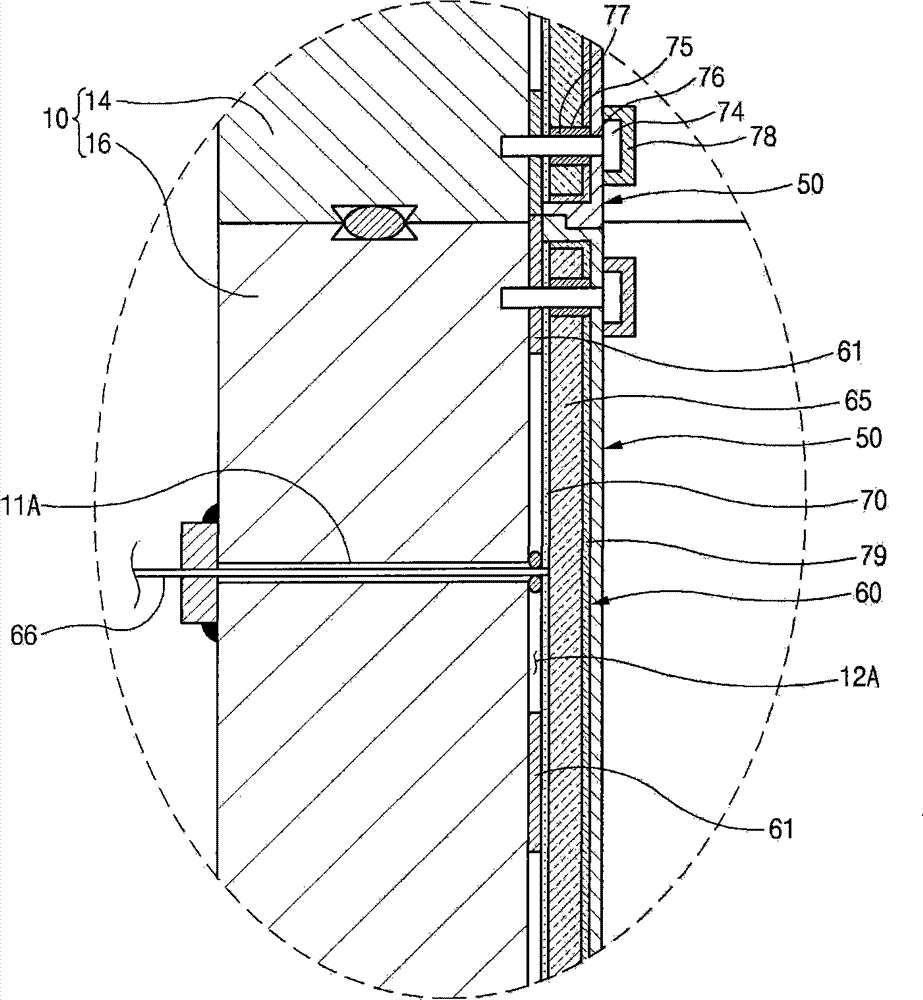
[0038] figure 1 is a cross-sectional view of a substrate processing apparatus according to a first embodiment of the present invention, figure 2 yes figure 1 A magnified view of part 'A' in , and image 3 and figure 2 Correspondingly, a substrate processing apparatus according to a second embodiment of the present invention is shown.

[0039] As shown, the substrate processing apparatus according to the first embodime...


PUM


Abstract

The invention discloses a substrate processing device, and particularly discloses a substrate processing device capable of performing scheduled working procedures of annealing, deposition, etching, and the like on a substrate. The substrate processing device comprises a cavity, a covering element and a temperature control element, wherein the cavity is used for forming a sealed processing space, the covering element is used for covering at least one part of the inner surface of the cavity, and the temperature control element is arranged between the covering element and the cavity so as to control the temperature of the processing space conveniently.

Description

technical field [0001] The present invention relates to a substrate processing device, in particular to a substrate processing device capable of implementing predetermined procedures such as annealing, deposition and etching on a substrate. Background technique [0002] A substrate processing apparatus is an apparatus capable of performing predetermined processes such as preheating, annealing, deposition, and etching on a substrate while the inner space of the processing space-chamber is at atmospheric pressure or vacuum pressure. [0003] Such substrate handling devices have become larger as glass substrates such as those used in liquid crystal display (LCD) panels have become larger. [0004] It is important for a substrate processing apparatus to maintain a processing environment with an appropriate temperature so that the substrate can be processed efficiently. In order to control the temperature of the processing space in the chamber, the walls of the chamber are forme...

Claims


Application Information

Patent Timeline
Patent Type & Authority Patents(China)
IPC IPC(8): H01L21/00
Inventor 崔日权
Owner WONIK IPS CO LTD
Why Eureka
Try Eureka