Vertical geometry light emitting diode package aggregate and production method of light emitting device using the same

a technology of vertical geometry and light emitting diodes, which is applied in the manufacture of semiconductor/solid-state devices, semiconductor devices, electrical devices, etc., can solve the problems of poor productivity of type, easy high temperature of packaging, and wiring disconnection, so as to facilitate temperature control and enhance the mass productivity of light emitting devices. , the effect of high strength

Inactive Publication Date: 2010-07-29
CI KASEI COMPANY
View PDF3 Cites 57 Cited by
  • Summary
  • Abstract
  • Description
  • Claims
  • Application Information

AI Technical Summary

Benefits of technology

[0021]In order to solve these problems, an object of the present invention is to provide an aggregate of vertical geometry light emitting diode packages each comprising a plurality of substrate portions insulated from each other by a slit, and a reflector adhered to the substrate portions to partially cover the slit, where the package aggregate has high strength, facilitates the temperature control in the production process of a light emitting device, and contributes to the enhancement of mass productivity of light emitting devices.
[0024]In the periphery of each package unit, a peripheral slit divided into a plurality of portions and / or at least one peripheral weakened part may be provided. The peripheral slit and / or peripheral weakened part makes it easy to separate one light emitting device or a group consisting of a required number of light emitting devices from an aggregate of light emitting devices produced by mounting vertical geometry light emitting diodes on respective package units.
[0025]In the periphery of each package unit, a plurality of leads as parts of the metal sheet, with one end being connected to the package unit, and a peripheral opening divided into a plurality of portions by the leads may also be provided. The peripheral opening of each package unit is effective in reducing the heat capacity of the package aggregate having formed therein a number of package units and makes it easy to control the temperature when producing light emitting devices by mounting vertical geometry light emitting diodes on the package aggregate.

Problems solved by technology

The vertical geometry light emitting diode allows a large current flow and enhanced illuminance, whereas the configuration of submounted type has a drawback that since heat generated from the diode can be hardly dissipated due to poor thermal conductivity, the package readily reaches a high temperature and this gives rise to occurrence of wiring disconnection or the like in the course of use.
In addition, the submounted type also has a problem of poor productivity.
(1) the thickness of the wiring material used is limited and a large current cannot be passed or if a large current is passed, the material in the periphery burns out,
(2) fluctuation is produced in the bonding strength of the wiring material and separation of the wiring material readily occurs,
(3) the joining part is weak to vibrations and a sealing material is necessary for reinforcement, and
(4) cracking is readily produced in the electrode of the light emitting diode or in the semiconductor layer due to ultrasonic oscillation and pressure during the connection and therefore, the apparatus used needs to be subtly adjusted.
If the temperature control is insufficient, this adversely affects the light emitting diode in many cases.

Method used


Image

  • Vertical geometry light emitting diode package aggregate and production method of light emitting device using the same
  • Vertical geometry light emitting diode package aggregate and production method of light emitting device using the same
  • Vertical geometry light emitting diode package aggregate and production method of light emitting device using the same

Examples


Embodiment Construction

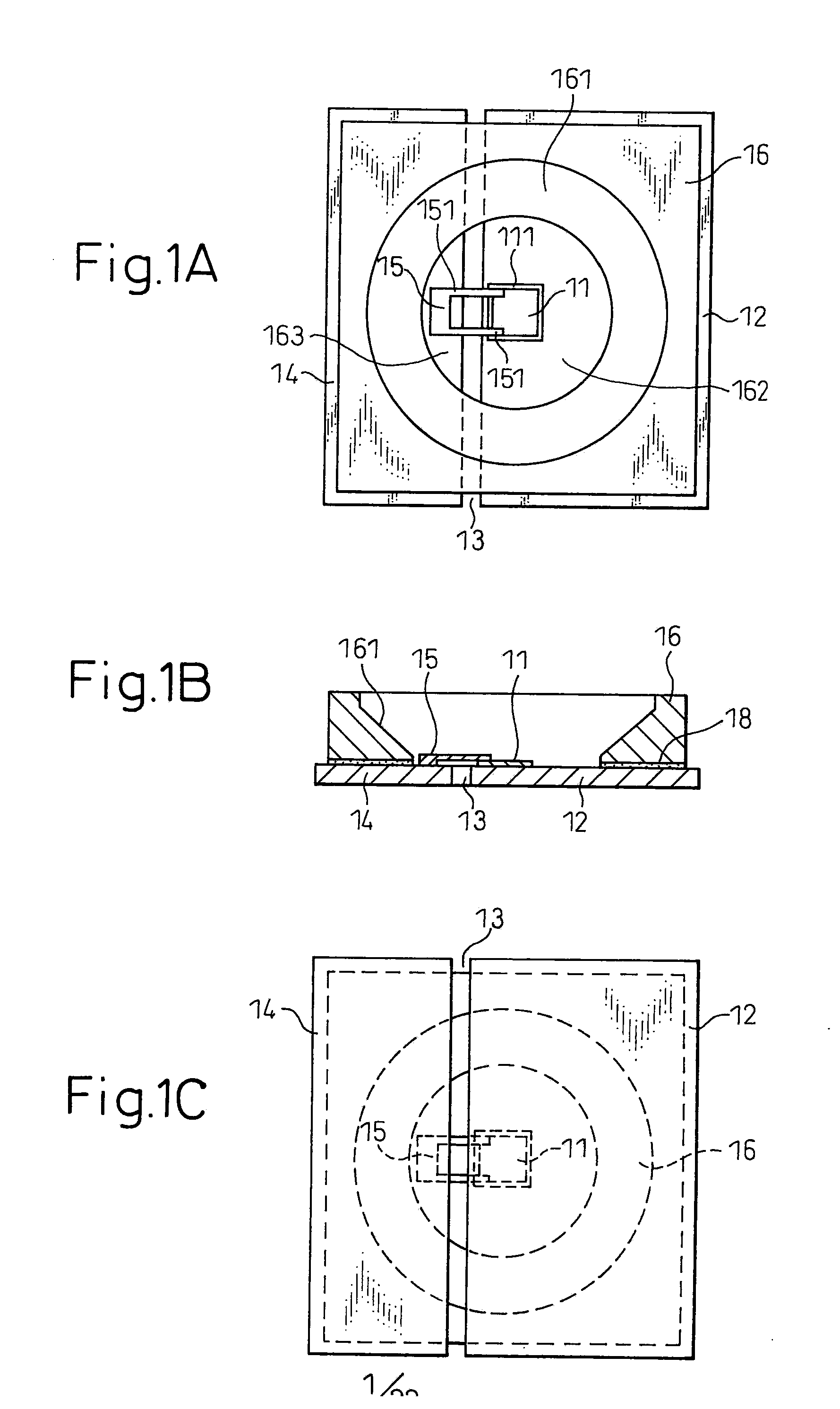
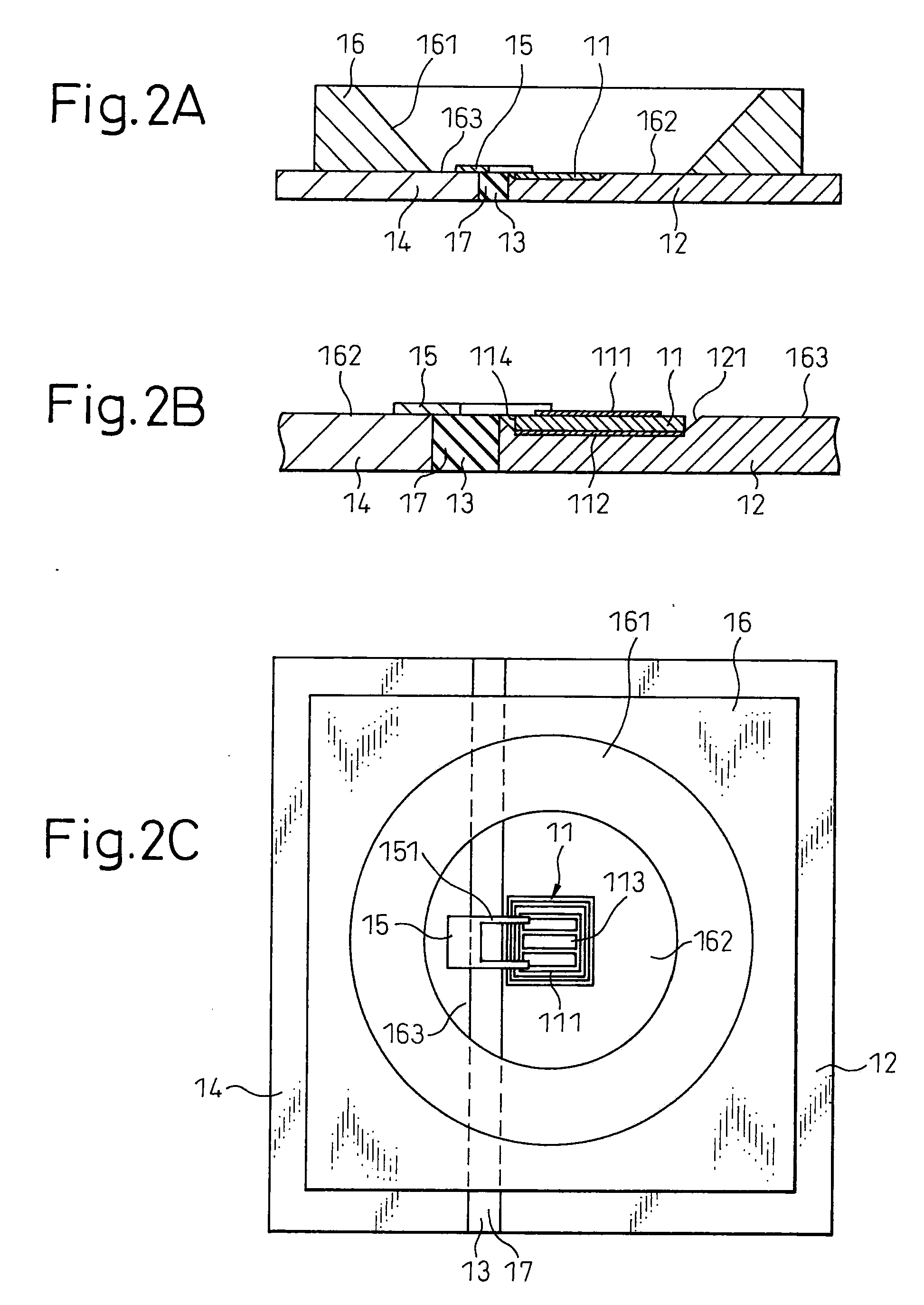
[0062]The vertical geometry light emitting diode package aggregate of the present invention is a vertical geometry light emitting diode package aggregate comprising a metal sheet having formed thereon a number of vertical geometry light emitting diode package units, each package unit comprising two or more substrate portions as parts of the metal sheet, which are separated by a slit, and a reflector having a penetrating opening and being adhered to the two or more substrate portions to cover parts of the slit such that the vertical geometry light emitting diode-mounting position is exposed in the inner side of the opening, and the end parts of the slit are exposed in the outer side of the reflector.

[0063]Before describing the vertical geometry light emitting diode package aggregate of the present invention in detail, the package unit working out to a unit in producing one light emitting device will be described by referring to FIGS. 1A to 1C. FIG. 1A is a plan view of the package un...


PUM


Abstract

There are provided a vertical geometry light emitting diode package aggregate useful for the production of a light emitting device having a vertical geometry light emitting diode as the light source, the light emitting device satisfying requirements in terms of current capacity flowed for light emission, dissipation of heat generated due to flow of a large current, resistance to thermal stress, strength of device and light emission efficiency, and a method for producing a light emitting device having a vertical geometry light emitting diode as the light source by using the package aggregate. The vertical geometry light emitting diode package comprises a metal sheet having formed thereon a number of vertical geometry light emitting diode package units, each package unit comprising two or more substrate portions as a part of the metal sheet, which are separated by a slit, and a reflector having a penetrating opening and being adhered to the two or more substrate portions to cover parts of the slit such that the vertical geometry light emitting diode-mounting position is exposed in the inner side of the opening and at the same time, the end part of the slit is exposed in the outer side of the reflector.

Description

TECHNICAL FIELD[0001]The present invention relates to a package for a vertical geometry light emitting diode provided with an upper electrode and a lower electrode. More specifically, the present invention relates to a vertical geometry light emitting diode package aggregate, which is an aggregate of packages before producing light emitting devices having a vertical geometry light emitting diodes as the light source and is suitable for the mass production of such light emitting devices. The present invention also relates to a method for producing a light emitting device having a vertical geometry light emitting diode as the light source by using the package aggregate of the present invention.BACKGROUND ART[0002]FIGS. 25A and 25B are a schematic drawing and an overhead view explaining a light emitting diode assembly in the form of a light emitting device of the prior art having a light emitting diode as the light source thereof. In FIGS. 25A and 25B, a light emitting diode assembly 6...

Claims


Application Information

Patent Timeline
Patent Type & Authority Applications(United States)
IPC IPC(8): H01L33/48H01L21/50H01L33/60H01L33/62H01L33/64
CPCH01L25/0753H01L33/60H01L33/62H01L33/64H01L2224/45014H01L2224/45144H01L2924/00014H01L33/647H01L2224/48H01L2924/00H01L2924/206
Inventor FUSHIMI, HIROSHINISHIYAMA, KENGOKUDOU, KOUJIYAMAMOTO, ITSUKIMITSUYAMA, KAZUMA
Owner CI KASEI COMPANY
Why Eureka
Try Eureka