Method and device for optimizing technological process

A technology of process flow and optimization method, which is applied in the direction of electrical components, semiconductor/solid-state device manufacturing, circuits, etc., can solve problems such as chip scrapping and increasing optimization costs, so as to reduce optimization costs, avoid wrong operations, and reduce the probability of chip scrapping Effect

Active Publication Date: 2011-10-19
SEMICON MFG INT (SHANGHAI) CORP +1
View PDF4 Cites 5 Cited by
  • Summary
  • Abstract
  • Description
  • Claims
  • Application Information

AI Technical Summary

Problems solved by technology

[0009] It can be seen that in the optimization method of the process flow provided by the prior art, the operator manually batches the wafers according to the paper of the operation steps of each process in the optimized process flow, and manually follows the steps of each process in the optimized process flow. The specific

Method used


Image

  • Method and device for optimizing technological process
  • Method and device for optimizing technological process
  • Method and device for optimizing technological process

Examples


Embodiment Construction

[0039] In order to make the object, technical solution and advantages of the present invention clearer, the solutions of the present invention will be further described in detail below with reference to the accompanying drawings and examples.

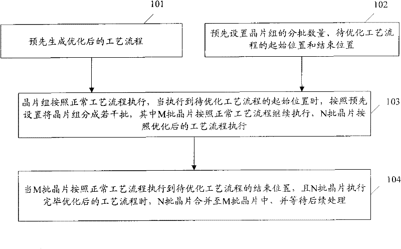
[0040] figure 1 It is a flow chart of the optimization method of the technological process provided by the present invention. Such as figure 1 As shown, the method includes the following steps:

[0041] Step 101, generating an optimized process flow in advance.

[0042] Specifically, generating an optimized process flow includes the following steps:

[0043] First, establish a general process flow, wherein the process parameters of each process in the general process flow are empty.

[0044] To establish a general process flow, the method for establishing a process flow in the prior art may be used, and details are not repeated here.

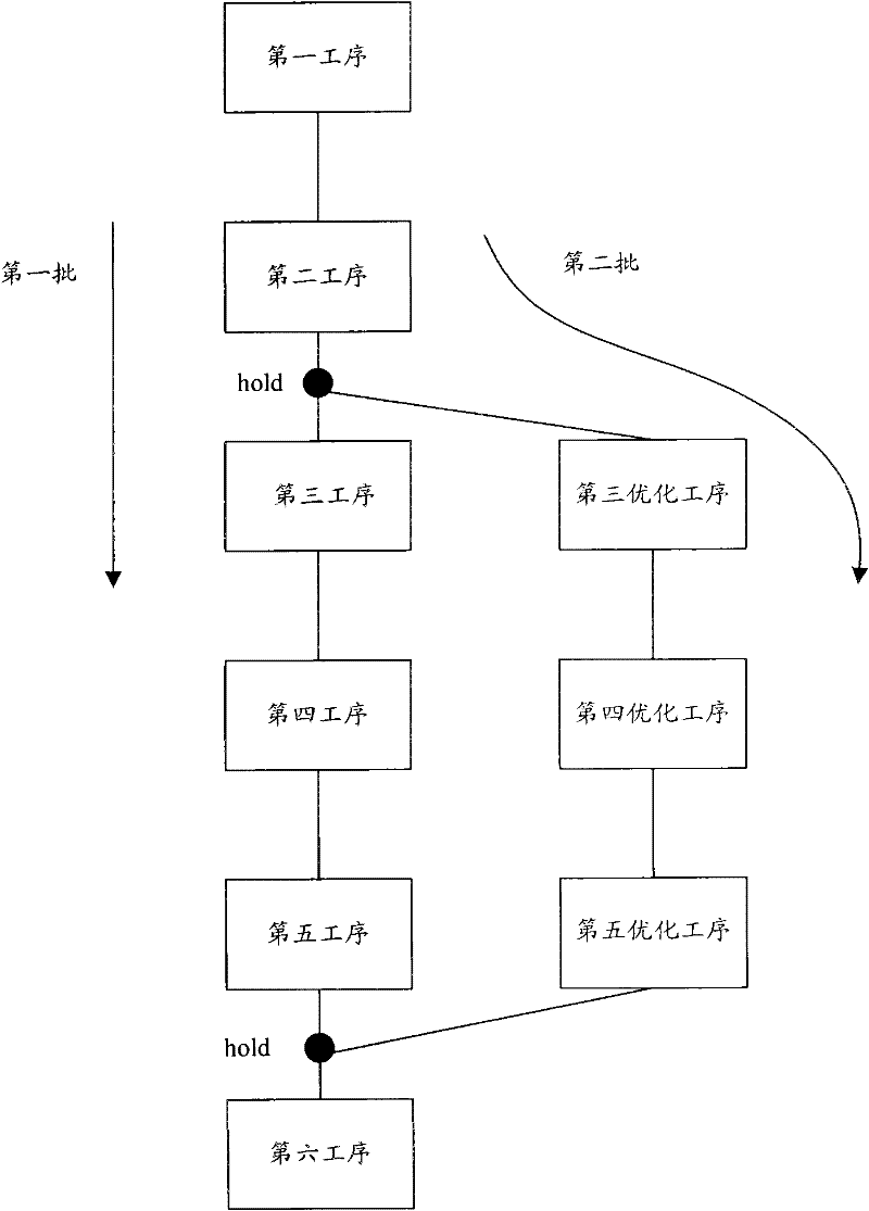
[0045] In the present invention, each process in the general process flow includes three sub-proc...


PUM


Abstract

The invention discloses a method for optimizing a technological process. An optimized technological process is produced in advance, and the number of batches of wafer sets and a starting position and an ending position of a technological process to be optimized are preset. The method comprises the following steps: the wafer sets are carried out according to a normal technological process, when the wafer sets are carried out to the starting position of the technological process to be optimized, the wafer sets are separated into a plurality of batches according to a preset valve, wherein M batches of wafer sets are continuously carried out according to the normal technological process, N batches of wafer sets are carried out according to the optimized technological process, and M and N are positive integers more than or equal to 1; when the M batches of wafer sets are carried out to the ending position of the technological process to be optimized according to the normal technological process, and the N batches of wafer sets are finished carrying out the optimized technological process, the N batches of wafer sets and the M batches of wafer sets are combined and wait for after-treatment. Meanwhile, the invention further discloses a device for optimizing the technological process; and with the adoption of the method and the device, the cost for optimizing can be lowered.

Description

technical field [0001] The invention relates to the field of integrated circuit manufacturing, in particular to a process flow optimization method and device. Background technique [0002] In the production and manufacture of integrated circuits, each wafer needs to go through hundreds or even thousands of processes from raw materials to final products, and all the processes that the wafer goes through constitute the process flow. Under normal circumstances, the wafer executes each process step by step according to the preset process flow, that is to say, the content of each process in the process flow is preset, and the content of each process also includes the specific process. The parameters also pre-set the time sequence for the execution of each process, and the process flow drive engine controls the chip to execute each process in sequence according to the pre-set process flow. [0003] However, in many cases, the wafer needs to be processed according to the optimized...

Claims


Application Information

Patent Timeline
IPC IPC(8): H01L21/00
Inventor 史晓霖王伦国隋云飞罗志林李延高雪清郭腾冲董海龙
Owner SEMICON MFG INT (SHANGHAI) CORP
Why Eureka
Try Eureka