Image sensor and manufacturing method thereof

A technology of image sensor and photosensitive unit, which is applied in the field of CMOS image processing, can solve problems such as optical crosstalk, and achieve the effect of avoiding optical crosstalk

Active Publication Date: 2013-05-01
GALAXYCORE SHANGHAI
View PDF1 Cites 0 Cited by
  • Summary
  • Abstract
  • Description
  • Claims
  • Application Information

AI Technical Summary

Problems solved by technology

[0006] The problem to be solved by the present invention is to provide an image sensor and its forming method, which solves the problem of optical crosstalk caused by the incident light reflected by the metal layer and entering the adjacent photosensitive unit in the existing image sensor

Method used


Image

  • Image sensor and manufacturing method thereof
  • Image sensor and manufacturing method thereof
  • Image sensor and manufacturing method thereof

Examples


Embodiment Construction

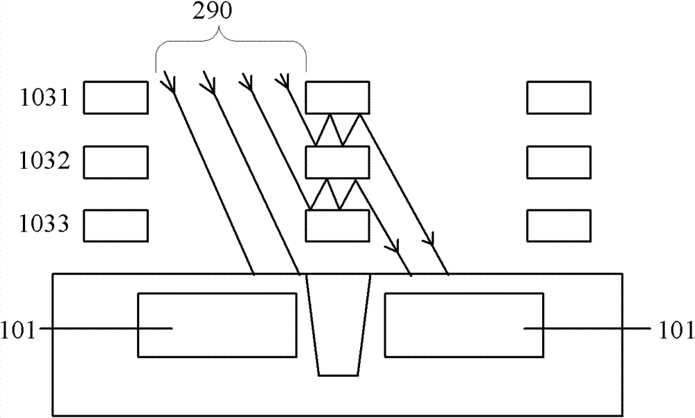
[0026] The inventors of the present invention found that in the existing image sensor, when the incident light is incident at a certain oblique angle, part of it reaches the photosensitive unit through the transparent interlayer dielectric layer, and the other part is irradiated on the metal layer and reflected. Since the position between the metal layers not connected by the conductive plugs is filled with a transparent interlayer dielectric layer, the incident light irradiated at this position is repeatedly reflected by the metal layer and finally enters other photosensitive units (usually adjacent photosensitive units). unit), forming optical crosstalk, which seriously affects the image display quality of the image sensor.

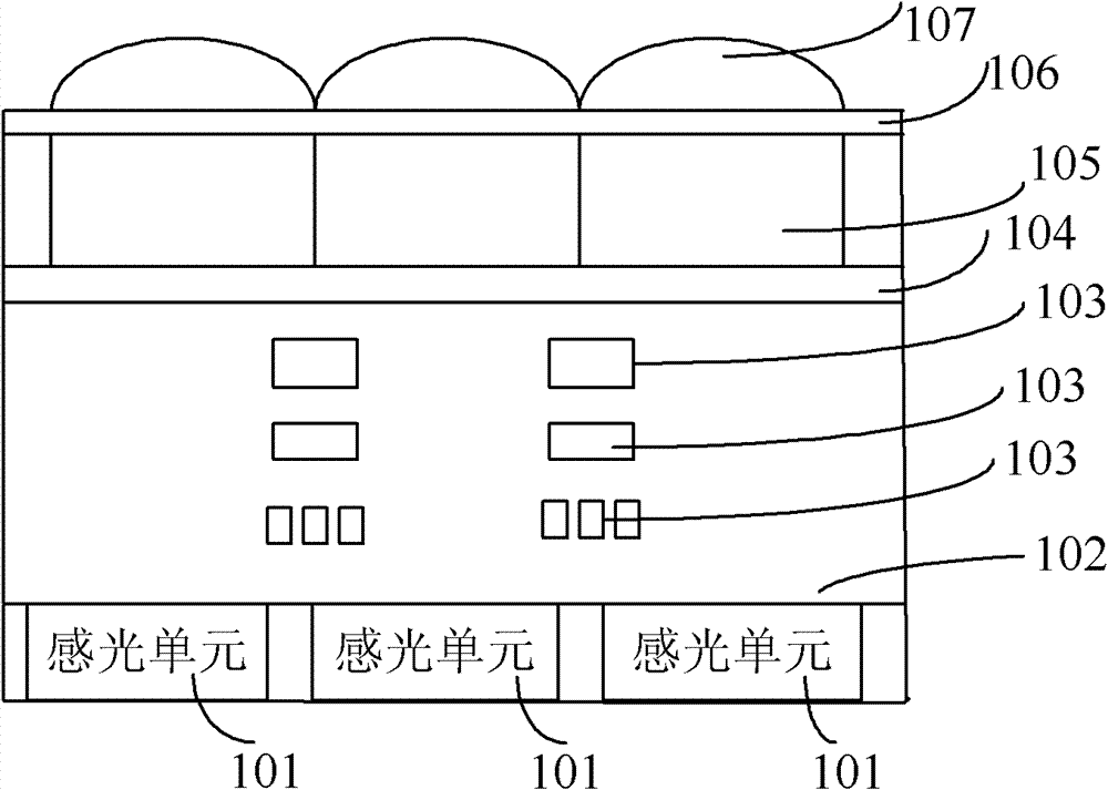
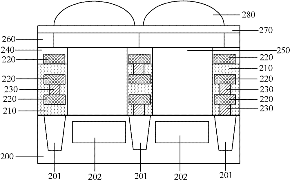
[0027] In view of the above-mentioned problems, the inventor, through research and analysis, proposes an image sensor, comprising: a semiconductor substrate, a pixel array is formed in the semiconductor substrate, the pixels include photosensitive units,...


PUM


Abstract

The invention relates to an image sensor and a manufacturing method thereof, wherein the image sensor comprises a semiconductor substrate, a euphotic layer, a lightproof layer, metal layers and a conductive plug. A pixel array is arranged in the semiconductor substrate, a pixel comprises a light sensitive unit, and adjacent pixels are separated by a low trench insulating structure; the euphotic layer is arranged on the surface of the semiconductor substrate and is aligned to the light sensitive unit; the lightproof layer is arranged on the surface of the semiconductor substrate and surrounds the euphotic layer; the metal layers are arranged in the lightproof layer; and the conductive plug is used for connecting adjacent metal layers. The image sensor can effectively prevent incident lightfrom entering other light sensitive units so as to avoid the generation of optical crosstalk, and the image display quality of pixels of the image sensor is improved.

Description

technical field [0001] The invention relates to the field of CMOS image processing, in particular to an image sensor and a method for forming the same. Background technique [0002] At present, image sensors have been widely used in cameras, medical equipment, cellular phones, automobiles and other occasions. The manufacturing process of image sensors, especially CMOS (Complementary Metal Oxide Semiconductor) image sensors (CIS), has made great progress, and it is constantly promoting the development of image sensors in the direction of high integration and miniaturization. Each pixel of an image sensor typically contains a light-sensitive element such as a photodiode and one or more transistors for reading signals from the light-sensitive element. CMOS image sensors use metal wires to connect each photosensitive unit to other photosensitive units and output terminals; these metal wires are generally distributed in different layers to connect to different parts of the trans...

Claims


Application Information

Patent Timeline
Patent Type & Authority Patents(China)
IPC IPC(8): H01L27/146
Inventor 李杰
Owner GALAXYCORE SHANGHAI
Why Eureka
Try Eureka