Strain engineered composite semiconductor substrates and methods of forming same
A composite substrate and semiconductor technology, applied in semiconductor devices, semiconductor/solid-state device manufacturing, electrical components, etc., can solve problems such as degradation and difficult film growth
- Summary
- Abstract
- Description
- Claims
- Application Information
AI Technical Summary
Problems solved by technology
Method used
Image

Examples
Embodiment approach
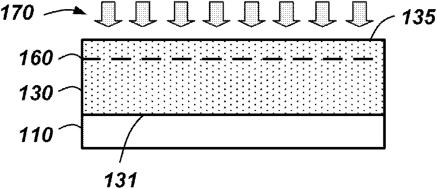
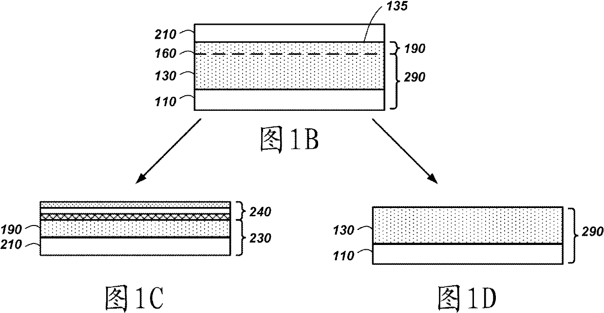
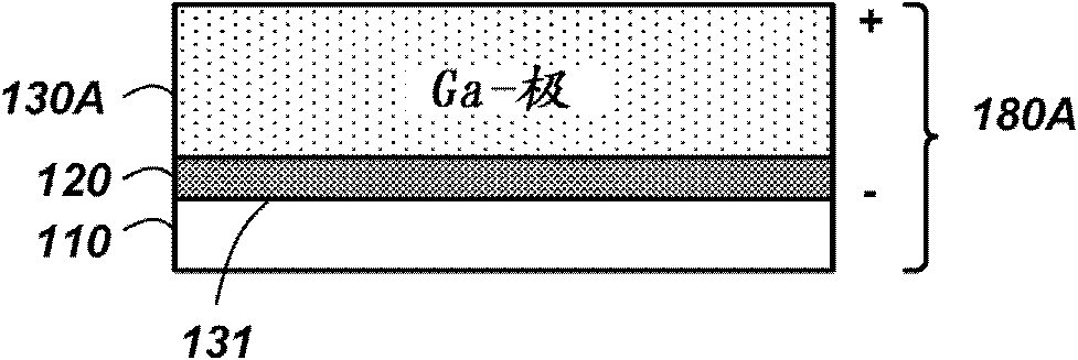
[0094] As a first example, an InGaN (or GaN) donor structure is formed. The example basically follows the Figure 3A-3G Actions and structures shown in . In this example, a sapphire growth substrate 110 was used. ZnO is deposited as a buffer layer 120 on the sapphire growth substrate 110 by means of, for example, MOVPE, HVPE or MBE.
[0095] On the surface of the ZnO buffer layer 120, lattice-matched In 0.18 Ga 0.82 N or strained GaN. The thickness of the nitride material can be kept below a critical thickness to prevent defect formation in the case of strained Ill-nitride material growth.
[0096] Use SiO 2 A sapphire carrier substrate 150 is bonded as a bonding layer to the surface of the strained Ill-nitride material 130 opposite the sapphire growth substrate 110 . Bonded structures can be strengthened by means of thermal annealing and / or using plasma activation as a pre-bonding surface treatment.
[0097] The back surface of the buffer layer 120 can be exposed by r...
PUM
| Property | Measurement | Unit |
|---|---|---|
| diameter | aaaaa | aaaaa |
| thickness | aaaaa | aaaaa |
| thickness | aaaaa | aaaaa |
Abstract
Description
Claims
Application Information
 - R&D Engineer
- R&D Manager
- IP Professional
- Industry Leading Data Capabilities
- Powerful AI technology
- Patent DNA Extraction
Browse by: Latest US Patents, China's latest patents, Technical Efficacy Thesaurus, Application Domain, Technology Topic.
© 2024 PatSnap. All rights reserved.Legal|Privacy policy|Modern Slavery Act Transparency Statement|Sitemap