Connector and manufacturing method thereof

A manufacturing method and connector technology, which are applied in the directions of connection, contact parts, circuit/collector parts, etc., can solve the problems of disappearance, shrinkage of solder balls 160, and high amount of gold, so as to reduce production costs, avoid solder creep, The effect of reducing the amount of gold

Active Publication Date: 2013-11-27
UNIMICRON TECH CORP
View PDF6 Cites 0 Cited by
  • Summary
  • Abstract
  • Description
  • Claims
  • Application Information

AI Technical Summary

Problems solved by technology

[0005] Since the gold layer 150 formed in the prior art needs to completely cover the portion of the second conductive layer 140 located in the through hole 116, the amount of gold used is relatively high, and the price of gold is quite expensive. Therefore, the production of the existing connector high cost
[0006] In addition, in the prior art, in order to increase the wiring density, the formation positions of the gold ring G and the solder ball 160 are usually very close to reduce the wiring area occupied by it. Therefore, when the solder ball 160 is formed, the solder is easy to contact the gold ring G. Ring G
However, when the solder is in contact with the gold ring G, there will be a phenomenon of solder wicking, so that the solder ball 160 shrinks or disappears.
In addition, in order to avoid contact with the gold ring G, the solder balls 160 need to be staggered with the gold ring G, so the distance between the solder balls 160 cannot be reduced

Method used


Image

  • Connector and manufacturing method thereof
  • Connector and manufacturing method thereof
  • Connector and manufacturing method thereof

Examples


Embodiment Construction

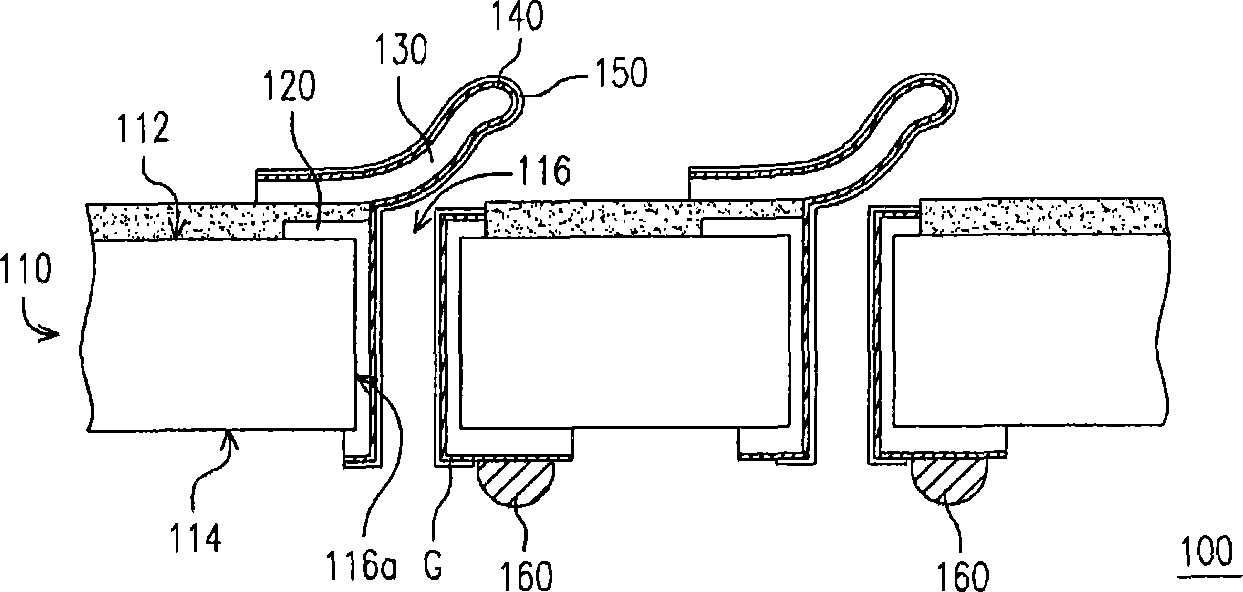
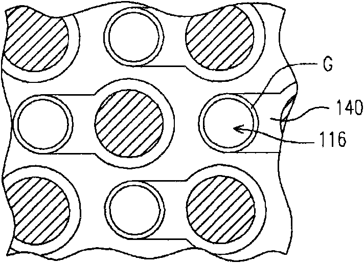
[0055] Figure 2A ~ Figure 2K A cross-sectional view of the manufacturing process of the connector according to an embodiment of the present invention is shown. Figure 3A A sectional view illustrating a connector according to an embodiment of the present invention, Figure 3B draw Figure 3A The bottom view of the connector.

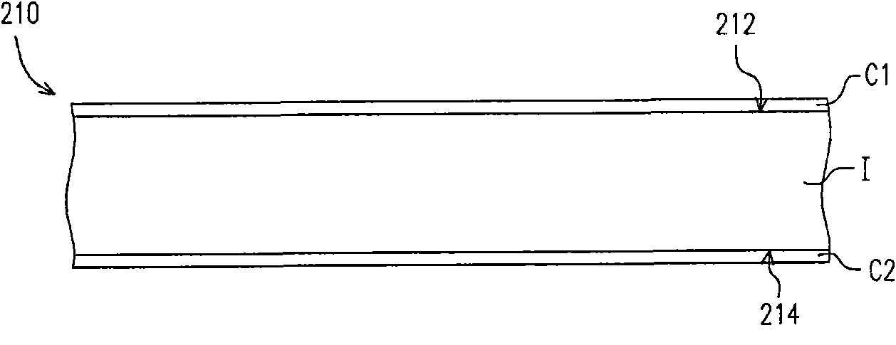
[0056] First, please refer to Figure 2A , provide a substrate 210, the substrate 210 has a first surface 212 and a second surface 214 opposite, wherein the substrate 210 is, for example, a double-sided board (a plate with a conductive layer on both sides of a single dielectric layer), a single-sided board ( A single dielectric layer has a conductive layer on one side), a single dielectric layer or a multi-layer board (multiple dielectric layers and multiple conductive layers stacked alternately).

[0057] In this embodiment, the substrate 210 is a double-sided board, and the substrate 210 includes a dielectric layer I and two conductive layers C1, ...


PUM


Abstract

The invention discloses a connector and a manufacturing method thereof. The method comprises the steps of: firstly, providing a substrate, wherein the substrate is provided with a first surface and a second surface which are opposite, and a through hole; secondly, forming a first electric-conductive layer on the substrate, wherein the electric-conductive layer covers the inner wall of the through hole; thirdly, filling a hole-plugging material in the through hole to form a hole-plugging column; fourthly, forming an electric-conductive elastic suspension arm on the first surface, and electrically connecting the electric-conductive elastic suspension arm with the first electric-conductive layer; fifthly, forming a gold-plated layer on the electric-conductive elastic suspension arm and the first surface, forming a solder ball on the second surface, and electrically connecting the solder ball with the first electric-conductive layer, wherein a free end part of the electric-conductive elastic suspension arm and the solder ball are positioned on a vertical line perpendicular to the first surface.

Description

technical field [0001] The present invention relates to a connector and its manufacturing method, and in particular to a connector with lower manufacturing cost and its manufacturing method. Background technique [0002] Generally speaking, an electronic device is usually equipped with a connector and has a connecting hole exposing the connector, so that external lines such as network cables or audio cables can be connected to the connecting hole by inserting them into the connecting hole The connector is electrically connected. [0003] Figure 1A showing a cross-sectional view of an existing connector, Figure 1B draw Figure 1A The bottom view of the connector. Please refer to Figure 1A , the existing connector 100 has a substrate 110 , a first conductive layer 120 , a plurality of connection terminals 130 , a second conductive layer 140 , a gold layer 150 and a plurality of solder balls 160 . The substrate 110 has a first surface 112 , a second surface 114 and a plur...

Claims


Application Information

Patent Timeline
Patent Type & Authority Patents(China)
IPC IPC(8): H01R43/00H01R13/02H01R13/03
Inventor 李长明刘文芳黄世荣苏铃凯
Owner UNIMICRON TECH CORP
Why Eureka
Try Eureka