Substrate cleaning device

A technology for cleaning devices and substrates, applied in cleaning methods and utensils, cleaning methods using liquids, electrical components, etc., can solve problems such as scattering, and achieve the effect of improving cleaning efficiency

Active Publication Date: 2011-12-21
TOKYO ELECTRON LTD
View PDF4 Cites 0 Cited by
  • Summary
  • Abstract
  • Description
  • Claims
  • Application Information

AI Technical Summary

Problems solved by technology

[0008] However, the technology described in Patent Document 1 has the following problem. Since a groove-shaped recess opening to the outer periphery is provided on the cleaning surface of the cleaning member, the cleaning liquid discharged from the groove-shaped recess is scattered toward the outer periphery during the cleaning process and hits the cover. Part of the cleaning fluid bounces back to produce a spray that will adhere to the wafer surface again

Method used


Image

  • Substrate cleaning device
  • Substrate cleaning device
  • Substrate cleaning device

Examples


no. 1 approach

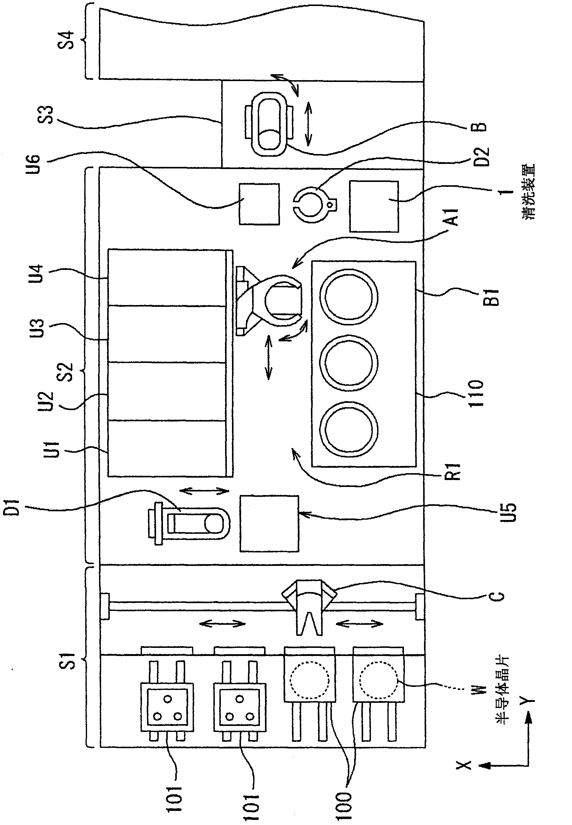
[0077] Figure 4 It is a perspective view (a) of the cleaning device 1 and an enlarged perspective view (b) of part I of (a), Figure 5 is a plan view of the cleaning device 1, Figure 6 is a longitudinal sectional view of the cleaning device 1 .

[0078] The cleaning device 1 adopts the following structure, and is installed on the box-shaped lower cover 40 with the upper surface open: the wafer W received from the above-mentioned second delivery arm D2 in the resist solution coating and development processing system is held approximately horizontally as the first wafer W. the suction pad 10 of the substrate holding unit; the spin chuck 20 functioning as the second substrate holding unit that receives the wafer W from the suction pad 10 and then holds the wafer W approximately horizontally in the same manner; and cleaning of the back surface of the wafer W Part 30.

[0079] Such as Figure 4 As shown, two adsorption pads 10 are provided in the cleaning device 1, and each a...

no. 2 approach

[0112] Figure 19 It is a schematic cross-sectional view showing a second embodiment of the cleaning device of the present invention.

[0113] The second embodiment is a case where the particles removed by the cleaning member 30 and the cleaning liquid used for cleaning are actively discharged. That is, if Figure 19 As shown, the drain pipe 81 is communicated (connected) with each discharge hole 36 provided in the cleaning unit 30, and the drain pipe 81 is connected with the suction pump 80 as a suction unit to actively discharge the particles removed by the cleaning unit 30. and cleaning fluid for cleaning. In this case, the servo motor 39 which is the rotation mechanism of the suction pump 80 and the cleaning member 30, and the flow rate adjustment valve 53 provided in the cleaning liquid supply pipe 51 are electrically connected to the controller 70 as a control unit, and based on the The control signal is controlled. In addition, in 2nd Embodiment, other parts are the...


PUM


Abstract

The present invention provides a substrate cleaning apparatus, comprising a keeping unit for holding a substrate horizontally and rotating around a vertical shaft, a cleaning member capable of rotating around the vertical shaft, a rotation mechanism for making the cleaning member to rotate, and a moving mechanism for driving the cleaning member move along a surface to be cleaned of the substrate, wherein the cleaning member is pasted with a spongy cleaning base part on a base part, the base part and the central part of the cleaning bottom are provided with discharge outlets connected with a cleaning liquid supply source, the surface of the cleaning bottom is provided with a basic end communicated with the cleaning liquid discharge outlets, a front end extends to a plurality of communicating grooves locating on front of the circumference of the cleaning member, and discharge holes communicated with the communicating grooves are arranged on position wherein the communicating grooves are located in the base part and one or more guide grooves communicated with the adjacent communicating grooves are located on the concentric circle of the cleaning surface of the cleaning bottom.

Description

[0001] This case is filed on June 4, 2009 , the application number is 200910142799.7 , the name of the invention is Substrate cleaning device divisional application technical field [0002] The present invention relates to a substrate cleaning device for cleaning and removing particles adhering to the surface of a substrate such as a semiconductor wafer or an FPD (Flat Panel Display) substrate. Background technique [0003] In general, in the manufacturing process of semiconductor devices, photolithography is used to form electrode patterns on semiconductor wafers, FPD substrates, etc. (hereinafter referred to as wafers, etc.). In this photolithography technique, a photoresist solution is applied to a wafer or the like by spin coating, the thus formed resist film is exposed according to a predetermined circuit pattern, and the exposed pattern is developed to obtain A circuit pattern is formed on the resist film. [0004] In addition, in the manufacturing process of semi...

Claims


Application Information

Patent Timeline
Patent Type & Authority Applications(China)
IPC IPC(8): H01L21/02B08B3/04
CPCB08B3/04H01L21/67051
Inventor 锦户修一吉高直人德永容一
Owner TOKYO ELECTRON LTD
Why Eureka
Try Eureka