Printed circuit board and method for controlling impedance of through hole structure on same

A printed circuit board and reference structure technology, applied in the direction of printed circuit components, etc., can solve the problems that the device cannot be installed, cannot be realized, and the diameter of the mounting hole and the relative position of the crimping component cannot be changed. The effect of changing impedance and avoiding adverse effects

Inactive Publication Date: 2011-12-21
RUIJIE NETWORKS CO LTD
View PDF3 Cites 10 Cited by
  • Summary
  • Abstract
  • Description
  • Claims
  • Application Information

AI Technical Summary

Problems solved by technology

[0008] The problem with the former method is that not only need to have enough space to design the reference structure of the through hole, but also for the installation hole of the crimping component, because this method often needs to set a relatively small space between the via structure and the reference structure. The large distance makes it impossible

Method used


Image

  • Printed circuit board and method for controlling impedance of through hole structure on same
  • Printed circuit board and method for controlling impedance of through hole structure on same
  • Printed circuit board and method for controlling impedance of through hole structure on same

Examples


Embodiment Construction

[0036] The following will clearly and completely describe the technical solutions in the embodiments of the present invention with reference to the accompanying drawings in the embodiments of the present invention. Obviously, the described embodiments are only some, not all, embodiments of the present invention. Based on the embodiments of the present invention, all other embodiments obtained by persons of ordinary skill in the art without creative efforts fall within the protection scope of the present invention.

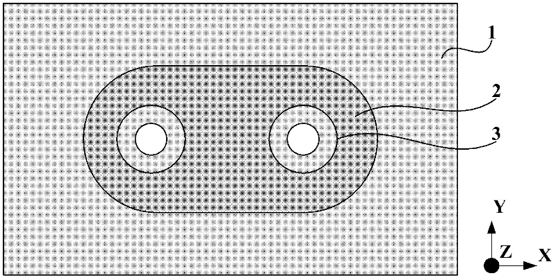
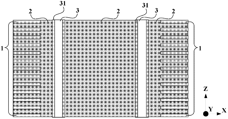
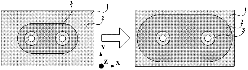
[0037] A printed circuit board provided by an embodiment of the present invention includes at least two through-hole structures, wherein the dielectric between the at least two through-hole structures is provided with non-metallized holes or non-metallized grooves, that is, hole walls or A through-hole or slot structure in which no metal is attached to the slot walls.

[0038] In this embodiment, the printed circuit board changes the equivalent dielectric constant ...


PUM


Abstract

The invention relates to a printed circuit board and a method for controlling the impedance of a through hole structure on the same. In the method, an equivalent dielectric constant between through hole structures or between the through hole structure and a reference structure is changed by a nonmetal hole or a nonmetal groove formed on a dielectric between at least two through hole structures or between the through hole structure and the reference structure, the impedance of the through hole structure is further changed, and negative influence caused by increasing a distance between the through hole structure and the reference structure in the prior art on the wiring of other lines of the circuit board is avoided. Therefore, the purpose that the impedance of the through hole structure in the high-density and high-power printed circuit board can be controlled and is free from the technological level can be achieved.

Description

technical field [0001] The invention relates to printed circuit board technology, in particular to a printed circuit board and a method for controlling the impedance of a through-hole structure on the printed circuit board. Background technique [0002] In printed circuit boards, there are many reasons that affect the quality of long-distance transmission signals, but in the final analysis it is caused by loss. The two fundamental factors that cause loss are dielectric loss and impedance mismatch during transmission. [0003] The so-called dielectric loss, that is, because the signal needs to be transmitted in a certain insulating environment such as vacuum, air or the dielectric between two conductive layers on the printed circuit board, but the dielectric is not a theoretical insulator, in practice, especially in Under the action of the alternating signal, part of the energy will flow back to the signal source through the dielectric, so that the signal energy in transmiss...

Claims


Application Information

Patent Timeline
IPC IPC(8): H05K1/02
Inventor 刘韡
Owner RUIJIE NETWORKS CO LTD
Why Eureka
Try Eureka