Display device, manufacturing method thereof, and active matrix substrate
A display device and display panel technology, which is applied in the directions of identification devices, nonlinear optics, optics, etc., can solve the problems such as the inability to supply display signals and the reduction of display quality.
- Summary
- Abstract
- Description
- Claims
- Application Information
AI Technical Summary
Problems solved by technology
Method used
Image
Examples
Embodiment approach 1
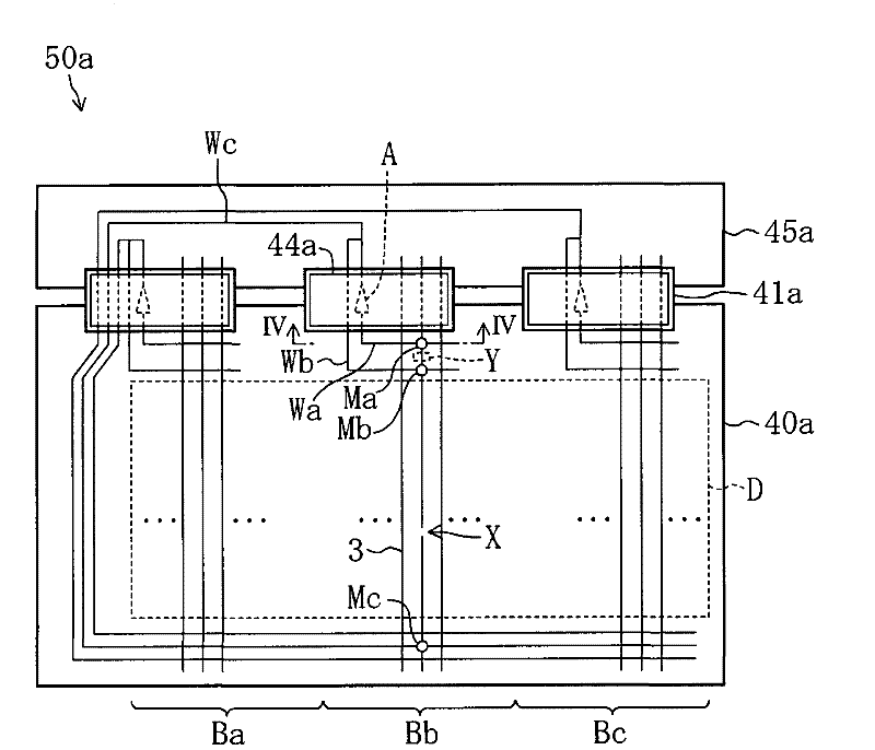
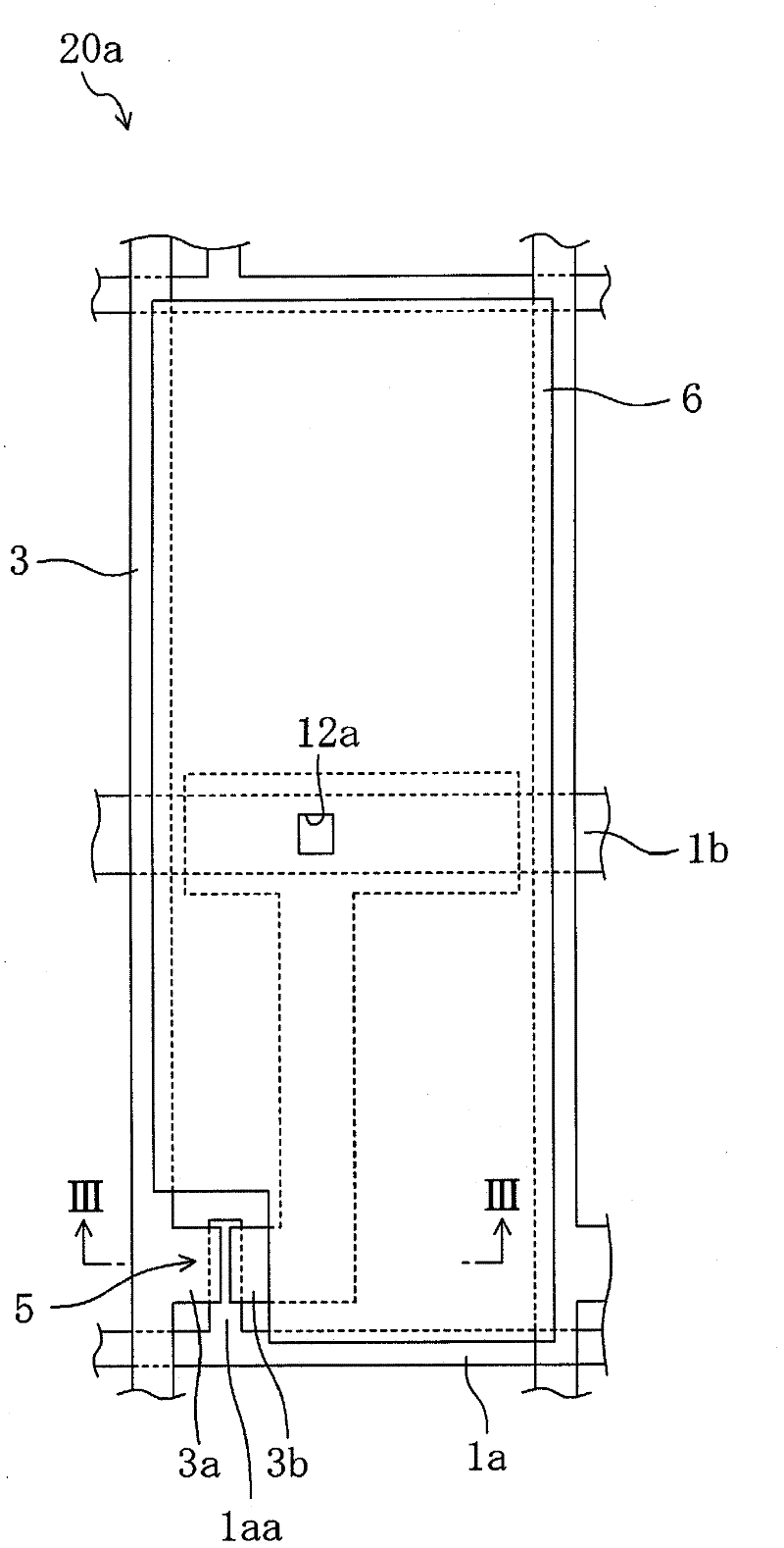
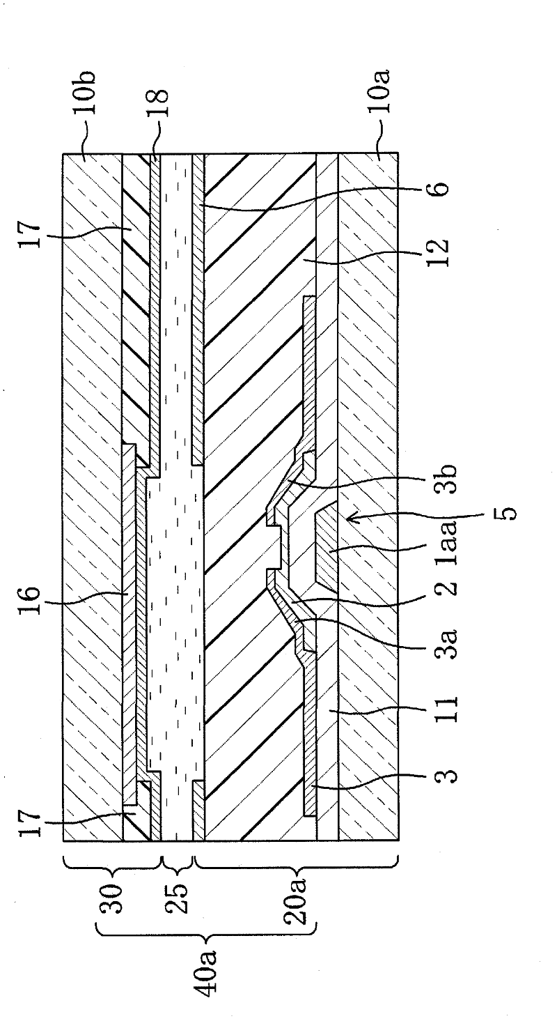
[0070] Figure 1 ~ Figure 4 Embodiment 1 of the display device, its manufacturing method, and active matrix substrate of the present invention is shown.
[0071] in particular, figure 1 It is a plan view of the liquid crystal display device 50a of this embodiment, figure 2 It is a plan view showing one pixel of the active matrix substrate 20a constituting the liquid crystal display device 50a. also, image 3 is along figure 2 A cross-sectional view of an active matrix substrate 20a on the line III-III and a liquid crystal display panel 40a having the active matrix substrate 20a, Figure 4 is along figure 1 A cross-sectional view of the active matrix substrate 20a along line IV-IV.
[0072] Such as figure 1 As shown, the liquid crystal display device 50a includes: a liquid crystal display panel 40a, three film substrates 41a respectively mounted on the upper end of the figure of the liquid crystal display panel 40a via ACF (Anisotropic Conductive Film, not shown), ...
Embodiment approach 2
[0127] Figure 5 It is a plan view of the liquid crystal display device 50b of this embodiment. In addition, in each of the following embodiments, for the Figure 1 ~ Figure 4 The same parts are denoted by the same symbols, and their detailed descriptions are omitted.
[0128] Such as Figure 5 As shown, the liquid crystal display device 50b includes: a liquid crystal display panel 40b, three film substrates 41b respectively mounted on the upper end of the figure of the liquid crystal display panel 40b via an ACF (not shown), and respectively mounted on an ACF (not shown). The printed circuit board 45b at the upper end in the figure of each film substrate 41b.
[0129] Such as Figure 5 As shown, the liquid crystal display panel 40b is substantially the same as the liquid crystal display panel 40a of Embodiment 1 except for the shapes of the wiring patterns of the first wiring path Wa, the second wiring path Wb, and the third wiring path Wc.
[0130] Such as Figure 5 As...
Embodiment approach 3
[0136] Figure 6 It is a plan view of the liquid crystal display device 50c of this embodiment. and, Figure 7 is a plan view of the load capacitance portion C constituting the liquid crystal display device 50c, Figure 8 It is a plan view of another load capacitance part C. also, Figure 9 is a plan view of the load resistance portion R constituting the liquid crystal display device 50c, Figure 10 It is a plan view of another load resistance part R. also, Figure 11 It is a plan view of the load resistance capacitance part E which comprises the liquid crystal display device 50c.
[0137] Such as Figure 6 As shown, the liquid crystal display device 50c includes: a liquid crystal display panel 40c, three film substrates 41a respectively mounted on the upper end of the figure of the liquid crystal display panel 40c via an ACF (not shown), and respectively mounted on an ACF (not shown). The printed circuit board 45a at the upper end in the figure of each film substrate ...
PUM
| Property | Measurement | Unit |
|---|---|---|
| thickness | aaaaa | aaaaa |
Abstract
Description
Claims
Application Information
 - R&D
- Intellectual Property
- Life Sciences
- Materials
- Tech Scout
- Unparalleled Data Quality
- Higher Quality Content
- 60% Fewer Hallucinations
Browse by: Latest US Patents, China's latest patents, Technical Efficacy Thesaurus, Application Domain, Technology Topic, Popular Technical Reports.
© 2025 PatSnap. All rights reserved.Legal|Privacy policy|Modern Slavery Act Transparency Statement|Sitemap|About US| Contact US: help@patsnap.com


