AI technical title is built by Patsnap AI team. It summarizes the technical point description of the patent document.
A solid-state imaging device and device technology, which can be used in TV system components, electrical components, image communication, etc., and can solve problems such as image quality degradation
Inactive Publication Date: 2012-01-11
SONY CORP
View PDF9 Cites 4 Cited by
Summary
Abstract
Description
Claims
Application Information
AI Technical Summary
This helps you quickly interpret patents by identifying the three key elements:
Problems solved by technology
Method used
Benefits of technology
Problems solved by technology
In this case, the image quality deteriorates significantly
Method used
Image
Click on the blue label to locate the original text in one second.
Reading with bidirectional positioning of images and text.
Examples
no. 1 example
[0045] 1. First embodiment (first exemplary configuration of CMOS image sensor (solid-state imaging device))
[0046] 2. Second embodiment (second exemplary configuration of CMOS image sensor (solid-state imaging device))
no. 3 example
[0047] 3. Third embodiment (third exemplary configuration of CMOS image sensor (solid-state imaging device))
[0048] 4. Fourth Embodiment (Exemplary Configuration of Camera System)
[0049]
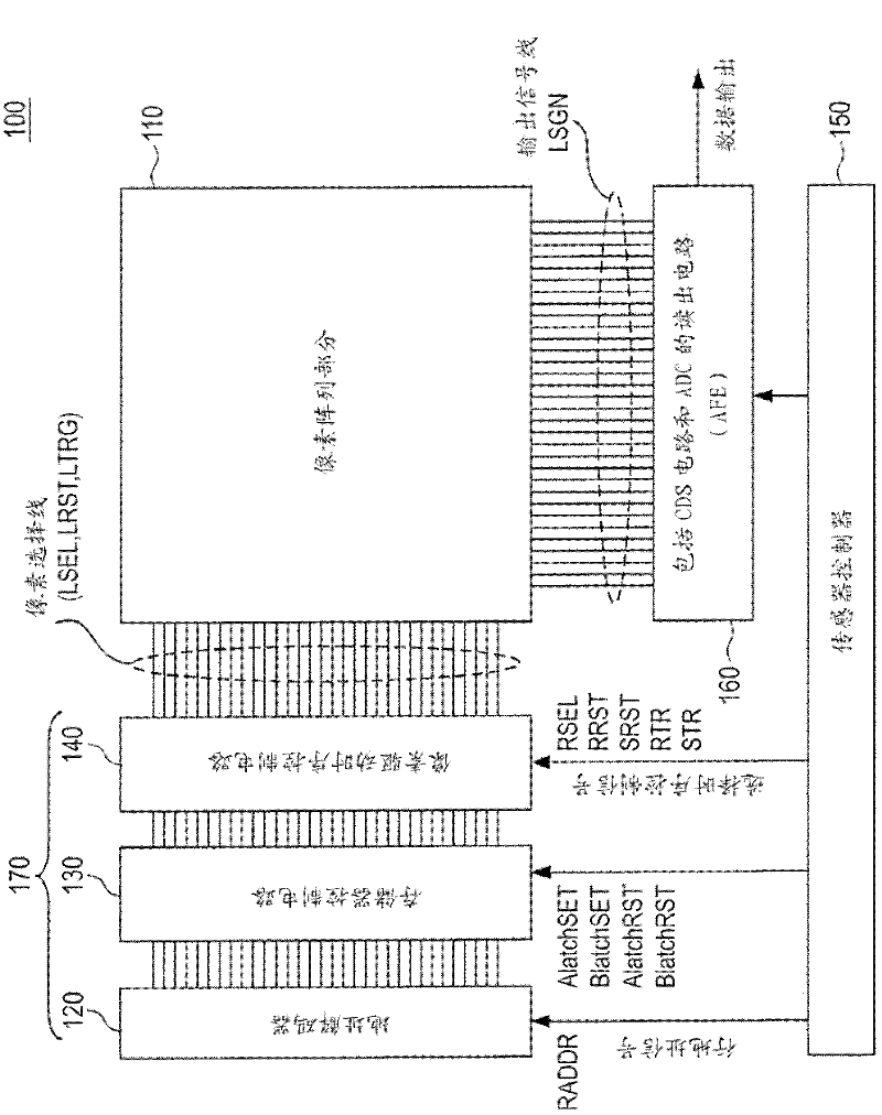
[0050] figure 1 Is a diagram illustrating an exemplary configuration of a CMOS image sensor (solid-state imaging device) according to the first embodiment of the present disclosure.
[0051] The CMOS image sensor 100 has a pixel portion 110, an address decoder 120, a latch (memory) control circuit 130, a pixel drive timing control circuit 140, a sensor controller 150, and a readout circuit (AFE) 160.
[0052] The address decoder 120, the memory control circuit 130, the pixel driving timing control circuit 140, and the sensor controller 150 constitute a pixel driving part.
[0053] In this embodiment, the address decoder 120, the memory control circuit 130, and the pixel drive timing control circuit 140 constitute a row (vertical) selection circuit 170.
[0054] The vertical selection circuit 170 is...
no. 2 example
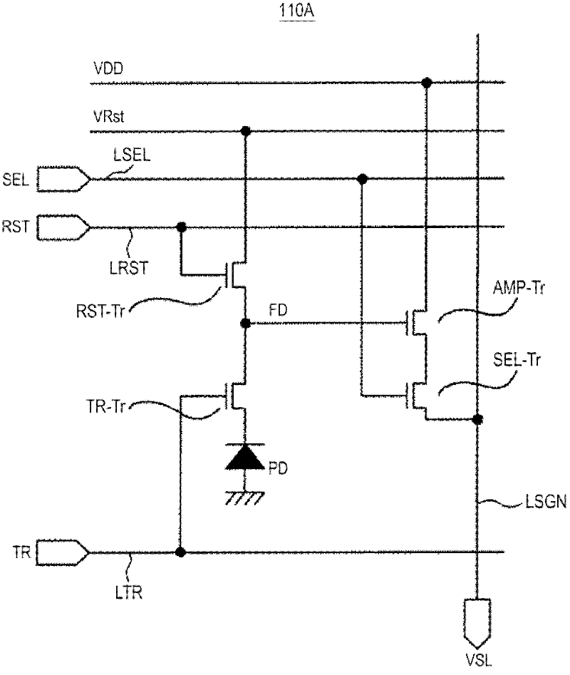
[0187] Picture 11 It is a diagram illustrating an example of a pixel drive timing control circuit and a memory control circuit of the vertical (row) selection circuit of the CMOS image sensor (solid-state imaging device) according to the second embodiment.
[0188] In the second embodiment, the circuit configuration is basically the same as that of the first embodiment.
[0189] Therefore, pixel drivers and other Figure 7 Or the same configuration as those of 8.
[0190] The second embodiment differs from the above-mentioned first embodiment in the following points. Such as Picture 11 As shown, the second memory (B memory) 132 of each row is reset as a whole by the B memory (latch) reset control signal BLatchRST.
[0191] in Picture 11 In the memory control circuit 130C, the AND gate AG134 is not arranged at the input stage of the reset terminal R of the second memory (B memory) 132, and directly provides the B memory (latch) reset control signal BLatchRST.
[0192] In the case of ...
PUM
Abstract
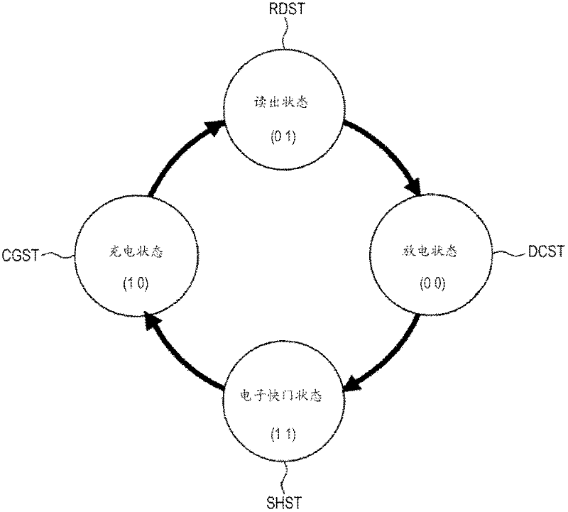
A solid-state imaging device includes: a pixel section wherein pixels including photoelectric conversion devices are arranged in a matrix; and a pixel driving section including a row selection circuit which controls the pixels to perform an electronic shutter operation and readout of the pixel section. The row selection circuit has a function of selecting a readout row from which a signal is read out and a shutter row on which reset is performed by discharging charge accumulated in the photoelectric conversion devices, in accordance with address and control signals. The row selection circuit can set, in accordance with the address and control signals, in the pixels of the selected row, at least a readout state, a discharge state where a smaller amount of the charge accumulated in the photoelectric conversion devices than the reset is discharged, an electronic shutter state, and a charge state where the charge is accumulated in the photoelectric conversion devices.
Description
Technical field [0001] The present invention relates to a solid-state imaging device and a camera system. Background technique [0002] Compared with a CCD (Charge Coupled Device) image sensor, a CMOS (Complementary Metal Oxide Semiconductor) image sensor (CIS) is characterized in that it is possible to set a readout address relatively freely. [0003] For example, its widely used sensor is a sensor that not only has the function of reading out all pixels of the sensor, but also has the "addition" that reads out the signals of multiple pixels at the same time. Functions such as "thinning-out" that reads out the signal intermittently at the same time, and "cutout" that reads only from some pixels. [0004] Sometimes "addition", "dilute" and "cut" can be executed simultaneously. [0005] In a sensor with functions of "addition", "dilute" and "cut", readout and shutter operations become complicated. Therefore, in most cases, for row selection, a decoder is used instead of a shift regis...
Claims
Application Information
Patent Timeline
Application Date:The date an application was filed.
Publication Date:The date a patent or application was officially published.
First Publication Date:The earliest publication date of a patent with the same application number.
Issue Date:Publication date of the patent grant document.
PCT Entry Date:The Entry date of PCT National Phase.
Estimated Expiry Date:The statutory expiry date of a patent right according to the Patent Law, and it is the longest term of protection that the patent right can achieve without the termination of the patent right due to other reasons(Term extension factor has been taken into account ).
Invalid Date:Actual expiry date is based on effective date or publication date of legal transaction data of invalid patent.

