Vacuum processing apparatus

A vacuum treatment device and vacuum treatment technology, which is applied in the direction of transportation and packaging, conveyor objects, electrical components, etc., can solve the problem of increasing the degree of control of the conveying rate, the throughput is not controlled, and the conveying speed cannot meet the requirements of the vacuum side. Problems such as substrate handling and handling, to achieve the effect of suppressing time and suppressing footprint tracks

Inactive Publication Date: 2012-01-25
TOKYO ELECTRON LTD
View PDF11 Cites 1 Cited by
  • Summary
  • Abstract
  • Description
  • Claims
  • Application Information

AI Technical Summary

Problems solved by technology

Therefore, in order to improve the throughput of the entire apparatus, for example, even if the processing time of each processing chamber is shortened, the shortened time may become the standby time of the processing chamber. becomes larger, it becomes difficult to improve throughput
[0006] Although Patent Documents 1 and 2 describe devices that perform processing in a vacuum atmosphere, they have not discussed the above-mentioned problems.
Although Patent Document 3 describes a technique of carrying in and carrying out a wafer W into and out of a processing chamber 40 using two transfer arms 45 a and 45 b in an air atmosphere, processing in a vacuum atmosphere has not been discussed.
In addition, although it is described in Patent Document 4 that by providing the processing units 31 to 35 around the transfer mechanism 30, the substrates are picked up by the arms 300 of the transfer mechanism 30 with respect to these processing units 31 to 35 almost simultaneously. Although the transfer time and throughput are not controlled, the transfer mechanism 30 needs a structure that rotates each arm 300, so the transfer mechanism 30 becomes larger.
[0007] Patent Documents 5 to 7 describe a load-lock structure for transferring substrates between the atmosphere side and the vacuum side. However, in this load-lock structure, the transfer speed of the transfer arm on the atmosphere side cannot satisfy the transfer and processing of the substrate on the vacuum side.

Method used


Image

  • Vacuum processing apparatus
  • Vacuum processing apparatus
  • Vacuum processing apparatus

Examples


Embodiment Construction

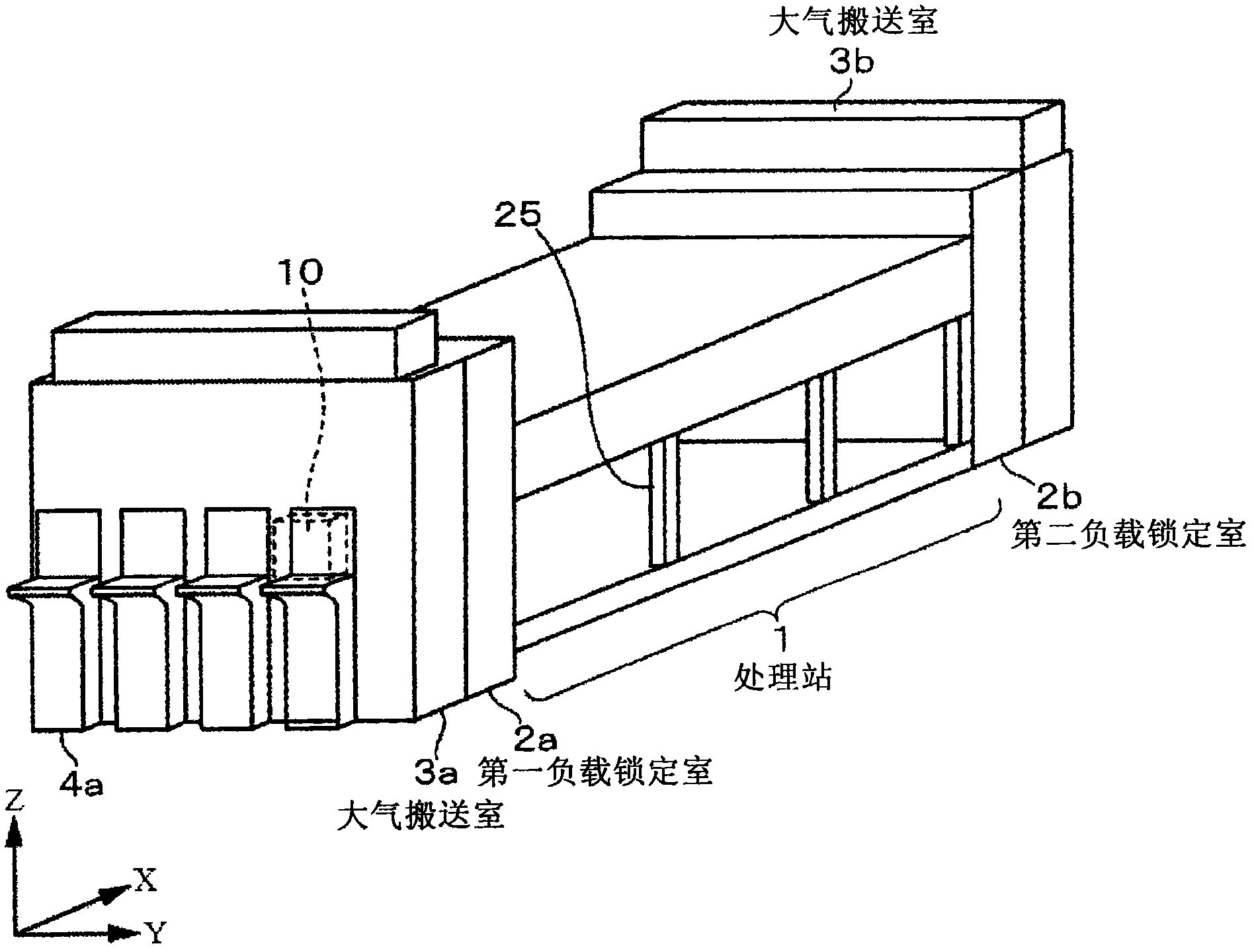
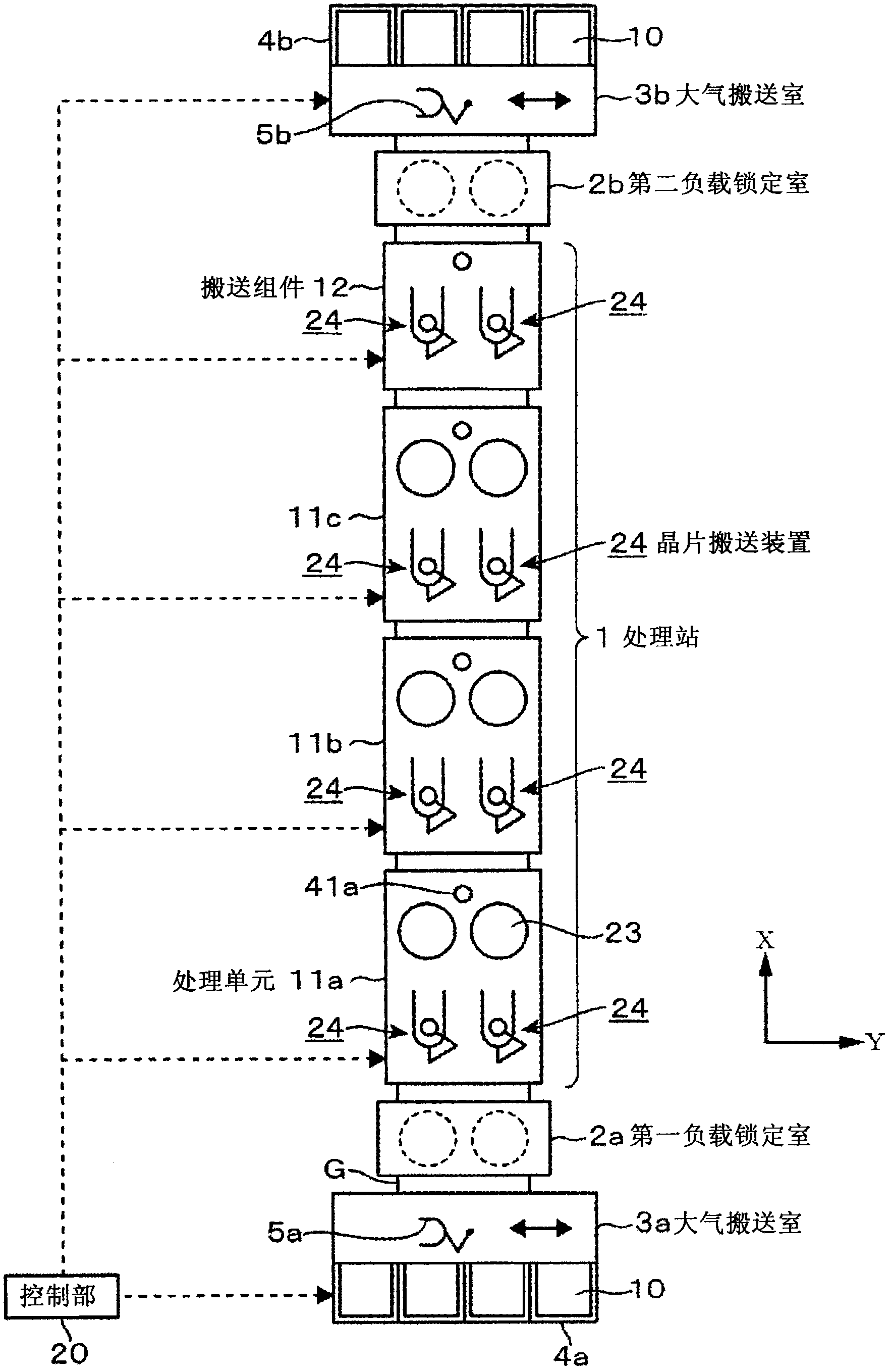
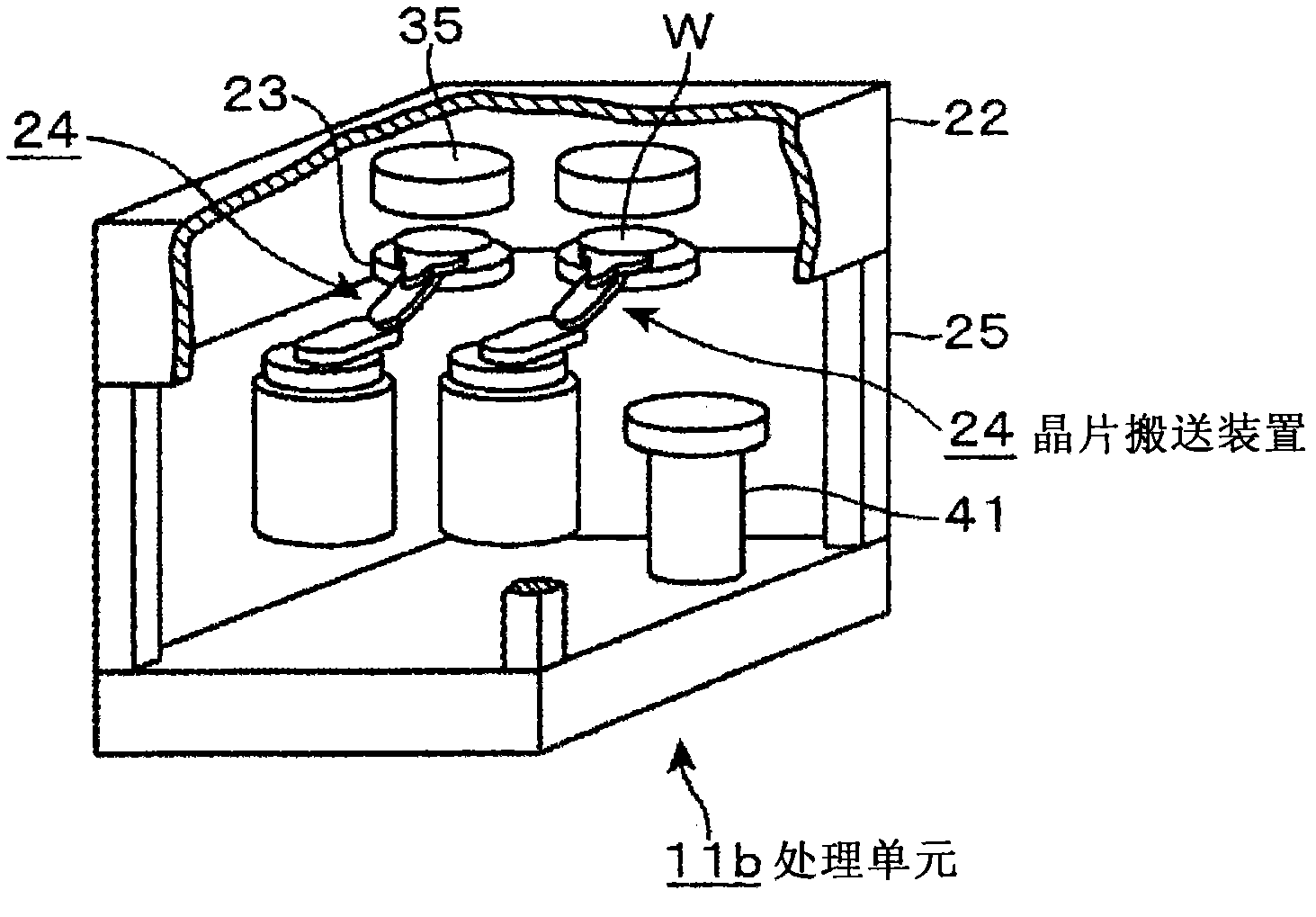
[0087] refer to Figure 1 to Figure 9 , an example of an embodiment of the vacuum processing apparatus of the present invention will be described. First, the overall structure of the vacuum processing apparatus will be described. The apparatus includes: a processing station 1 for processing a substrate, that is, a semiconductor wafer (hereinafter referred to as "wafer") W in a vacuum atmosphere. figure 1 and the first load-lock chamber 2a for carrying in and the second load-lock chamber 2b for carrying out, which are pre-vacuum chambers configured as follows: for opposing the processing station 1, respectively loading and unloading of the wafer W, with the processing station 1’s figure 2 One end side on the front side of the center and the other end side on the back side are respectively airtightly connected, and the internal atmosphere is switched between an atmospheric atmosphere and a vacuum atmosphere.

[0088] These load lock chambers 2a, 2b are configured so that two ...


PUM


Abstract

The invention provides a vacuum processing apparatus in which when vacuum processing is performed on substrates in a plurality of processing regions, it is possible to reduce an entire foot print of the apparatus and shorten the time between completion of vacuum processing on the substrates and starting of vacuum processing on next wafers in each of the processing regions. Three process units (11) and a transfer module (12) are sequentially and airtightly connected to each other in a row from the upstream side to the downstream side between load-lock chambers (2a, 2b). In addition, a wafer transfer device (24) is configured to transfer the wafer (W) to the process units (11) from one side of the upstream. The wafer transfer device (24) which is used to transfer the wafer (W) to the load-lock chamber (2b) from the process units (11) on one end of the downstream is arranged in a transfer module (12). The wafer (W) is transfered from the load-lock chamber (2a) to the process unit (11) on the upstream end. The wafer (W) is transfered from the load-lock chamber (2b) to the process unit (11) on the upstream end. The wafer (W) is transfered from the process unit (11a) on the upstream side to the process unit (11) on the downstream side.

Description

technical field [0001] The present invention relates to a vacuum processing device for vacuum processing a substrate. Background technique [0002] As a vacuum processing apparatus for vacuum processing substrates such as semiconductor wafers (hereinafter referred to as "wafers"), there is known: a plurality of processing chambers are radially connected to the side of a vacuum transfer chamber maintained in a vacuum atmosphere. A shared wafer transfer mechanism (transfer mechanism) installed in the transfer chamber to freely rotate around a vertical axis and freely move up and down, and to carry wafers in and out of these processing chambers is called a multi-chamber system and a cluster tool. installation. This wafer transfer apparatus is configured to include, for example, two pickers that support wafers from below to carry wafers in and out, respectively, and move a plurality of wafers into and out of the processing chamber sequentially by advancing, retreating, and rota...

Claims


Application Information

Patent Timeline
Patent Type & Authority Applications(China)
IPC IPC(8): H01L21/00H01L21/677
CPCH01L21/67736H01L21/67173H01L21/205H01L21/3065H01L21/68
Inventor 宫下哲也原正道水泽宁平田俊治
Owner TOKYO ELECTRON LTD
Why Eureka
Try Eureka