High-alignment-packaging-type lead frame and packaging structure thereof

A technology of lead frame and position sealing, applied in the direction of electrical components, electric solid devices, circuits, etc., can solve the problems of chip circuit function failure, increase the complexity and risk of the packaging process, lead crossing, etc., achieve low packaging cost, avoid unnecessary Symmetrical deformation, high reliability effect

Active Publication Date: 2014-05-14
WUXI CHINA RESOURCE MICRO ASSEMBLY TECH
View PDF5 Cites 1 Cited by
  • Summary
  • Abstract
  • Description
  • Claims
  • Application Information

AI Technical Summary

Problems solved by technology

[0007] figure 1 The LQFP lead frame shown is suitable for packaging a chip with a square shape and equally distributed bonding pads (Bonding Pad) on four sides. There are more bonding pads distributed on the side, and relatively few bonding pads distributed on the wide side, so it is necessary to connect the bonding pads on the edge of the long side of the chip to the inner leads of the lead frame corresponding to the wide side of the chip. On the feet, therefore, there will be crossovers at the corners of the chip, which must be avoided in the packaging process (may be cross-connected and cause the chip circuit function to fail)
In the prior art, in order to avoid the problems caused by lead crossing when packaging rectangular chips, a special arc bending process can be performed during bonding, but this will increase the complexity and risk of the packaging process

Method used


Image

  • High-alignment-packaging-type lead frame and packaging structure thereof
  • High-alignment-packaging-type lead frame and packaging structure thereof
  • High-alignment-packaging-type lead frame and packaging structure thereof

Examples


Embodiment Construction

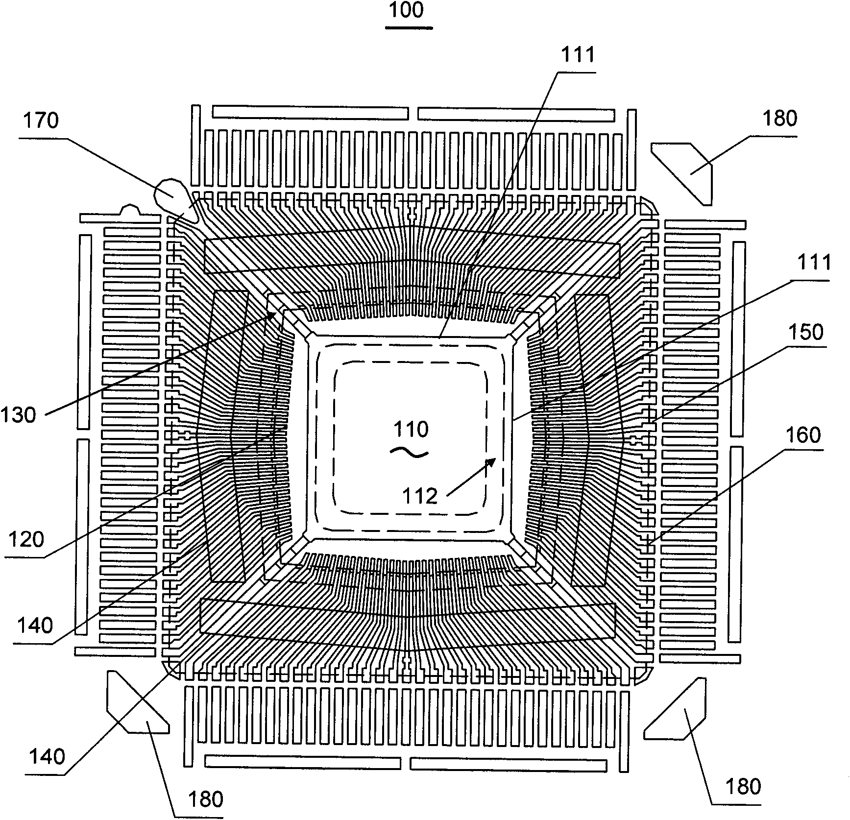
[0035] The following introduces some of the possible embodiments of the present invention, which are intended to provide a basic understanding of the present invention, but are not intended to identify key or decisive elements of the present invention or limit the scope of protection. In the drawings, for the sake of clarity, the thickness of layers or the area of ​​regions may be exaggerated, but as a schematic diagram, it should not be regarded as strictly reflecting the proportional relationship of geometric dimensions. In the drawings, the same reference numerals refer to the same structural parts, and thus their descriptions will be omitted.

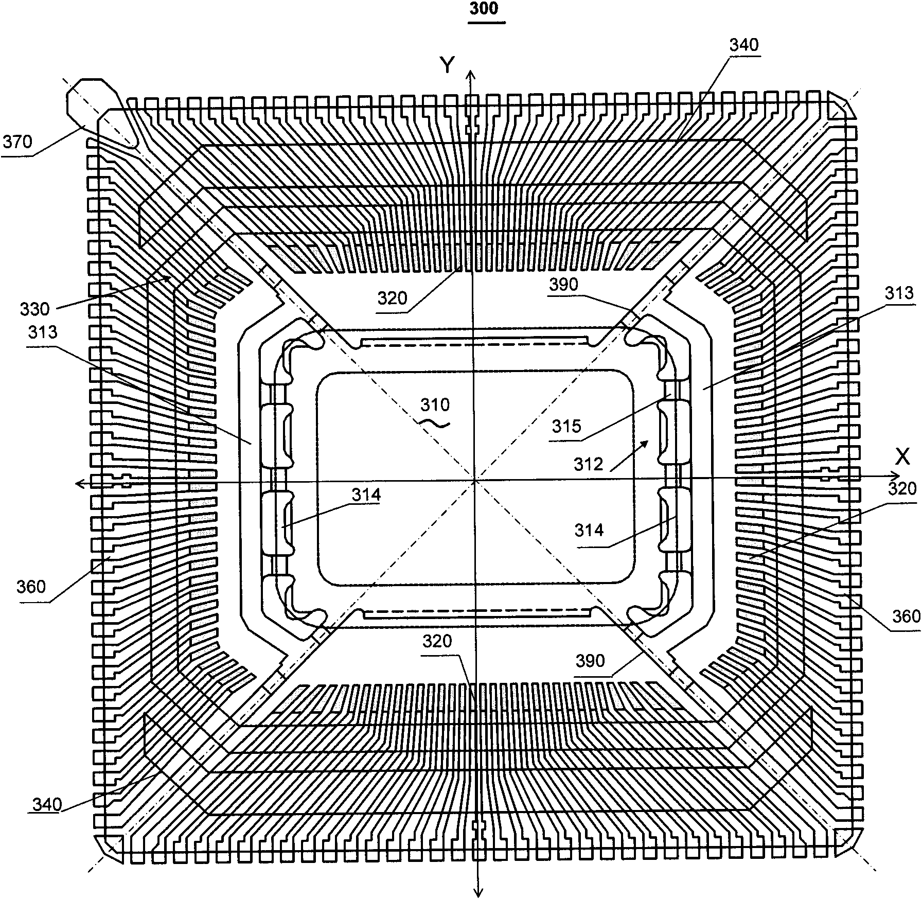
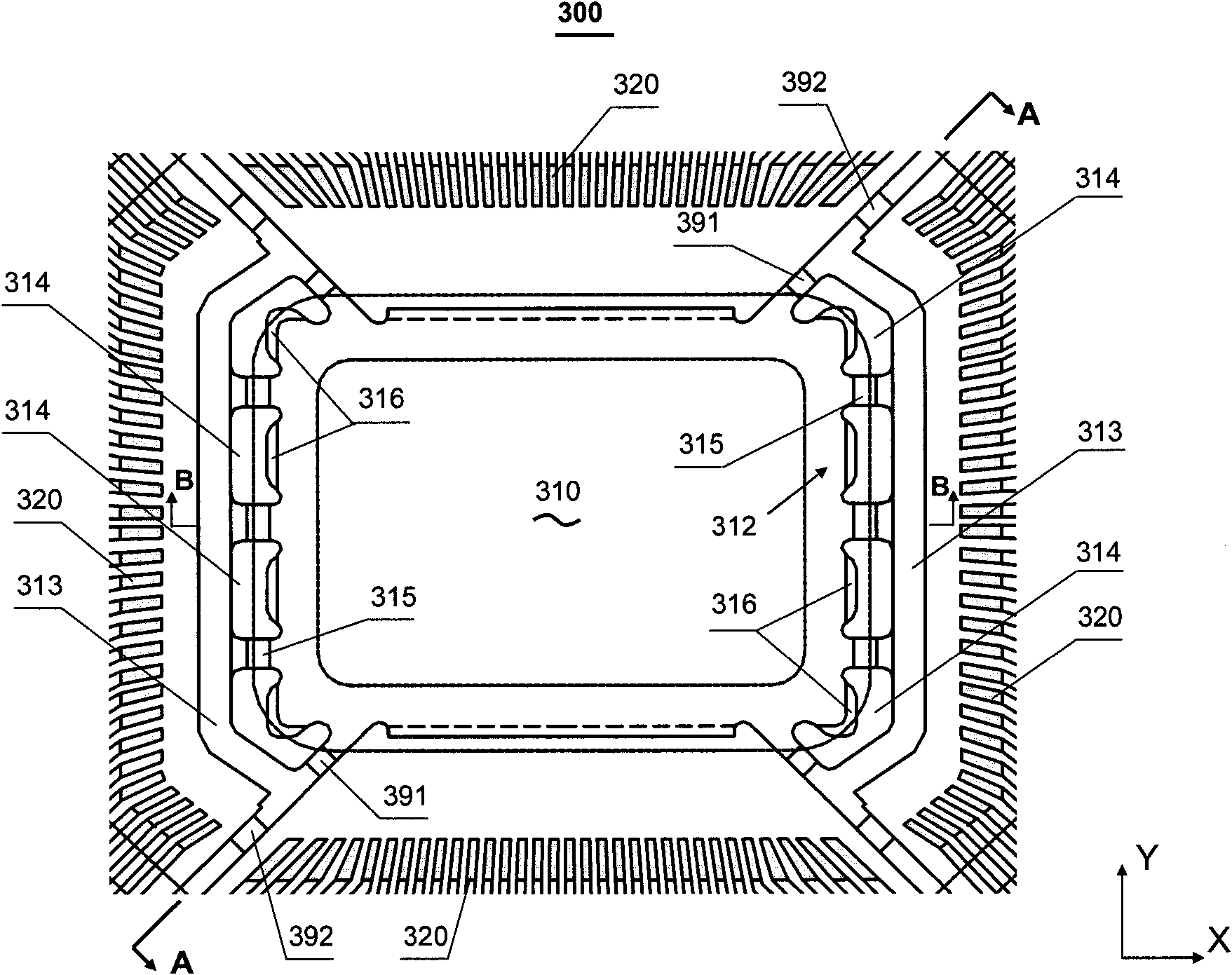
[0036] figure 2 Shown is a schematic structural view of a lead frame provided according to an embodiment of the present invention. image 3 shown as figure 2 Partial schematic of the central region of the leadframe shown.

[0037] First, if figure 2As shown, the lead frame 300 is a lead frame in the form of a high-wire packag...


PUM


Abstract

The invention provides a high-alignment-packaging-type lead frame and a packaging structure thereof, belonging to the technical field of chip packaging. The lead frame is square, is used for packaging a chip with bonding pads which are not equally distributed on four sides, and comprises a pad, inner pins, outer pins, pad connecting ribs and pad reinforcing rings which are fixedly connected between two pad connecting ribs. A lead frame array comprises a plurality of lead frames which are arranged in rows and lines. At the same time, the invention provides the packaging structure which comprises the lead frame. The lead frame can satisfy special packaging requirements on the chips with the bonding pads which are not equally distributed on four sides, the situation of gold wire intersection can be avoided during routing, the asymmetric deformation caused during plastic packaging can be also avoided, the reliability is high and the packaging cost is low.

Description

technical field [0001] The invention belongs to the technical field of chip packaging, in particular to a lead frame, in particular to a lead frame and a lead frame in the form of a high-wire package suitable for packaging a chip (chip die) with unequal numbers of bonding pads distributed on four sides Arrays and their packaging structures. Background technique [0002] Encapsulation is a very important step in the manufacturing process of electronic devices. Through the encapsulation process, various chips (chip die) can be directly drawn out of the circuit, so as to be electrically connected with external circuits. For various chips, the appropriate packaging form is usually selected. [0003] A package structure of a device generally includes a packaged chip, a lead frame and a package (usually a plastic package). Wherein, the lead frame is used to carry the chip and lead out the peripheral interface of the chip to form pins. In the prior art, corresponding to various ...

Claims


Application Information

Patent Timeline
Patent Type & Authority Patents(China)
IPC IPC(8): H01L23/495
CPCH01L2924/0002
Inventor 郑志荣仲学梅
Owner WUXI CHINA RESOURCE MICRO ASSEMBLY TECH
Why Eureka
Try Eureka