Dual-damascene structure and manufacturing method thereof

A dual damascene structure and manufacturing method technology, which is applied in semiconductor/solid-state device manufacturing, electrical components, electrical solid-state devices, etc., can solve the problems of dielectric constant change, low density, and low dielectric constant dielectric layer damage, etc., to prevent Effects of adverse effects, stable dielectric constant value, and improved reliability

Inactive Publication Date: 2012-03-14
SEMICONDUCTOR MANUFACTURING INTERNATIONAL (BEIJING) CORP +1
View PDF3 Cites 8 Cited by
  • Summary
  • Abstract
  • Description
  • Claims
  • Application Information

AI Technical Summary

Problems solved by technology

[0008] However, it is found in actual production that due to the low density of the low dielectric constant dielectric layer 110, when the chemical mechanical polishing process is used to remove the metal material on the low dielectric constant dielectric layer 110, the The used slurry (slurry) will react with the surface of the low dielectric constant dielectric layer 110, so that part of the thickness of the low dielectric constant dielectric layer is damaged, resulting in a change in the dielectric constant of the low dielectric constant dielectric layer, It will adversely affect the performance of the subsequently formed metal interconnection lines, thereby affecting the reliability of semiconductor devices

Method used


Image

  • Dual-damascene structure and manufacturing method thereof
  • Dual-damascene structure and manufacturing method thereof
  • Dual-damascene structure and manufacturing method thereof

Examples


Embodiment Construction

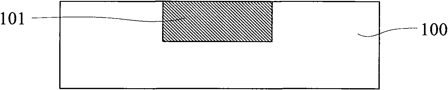
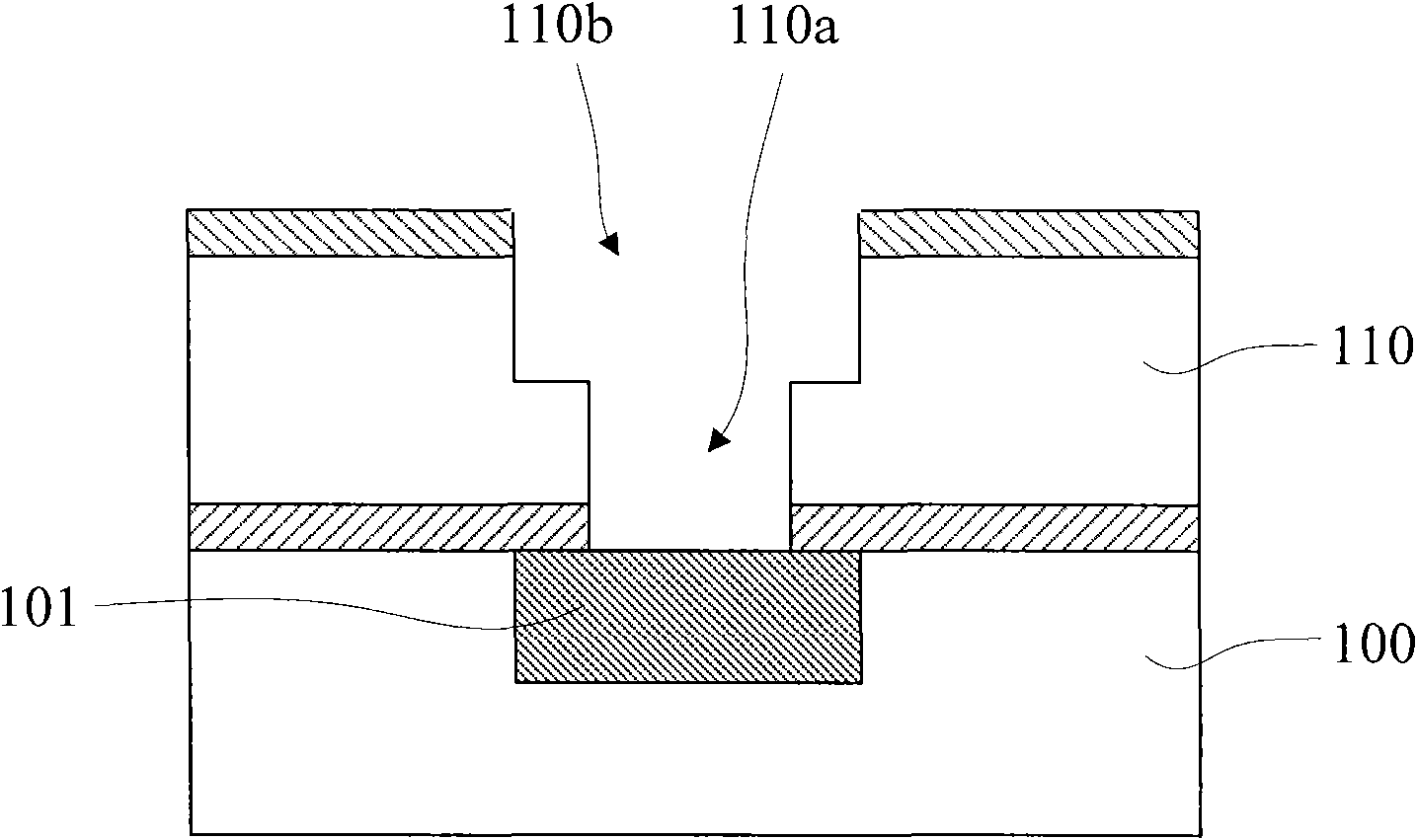
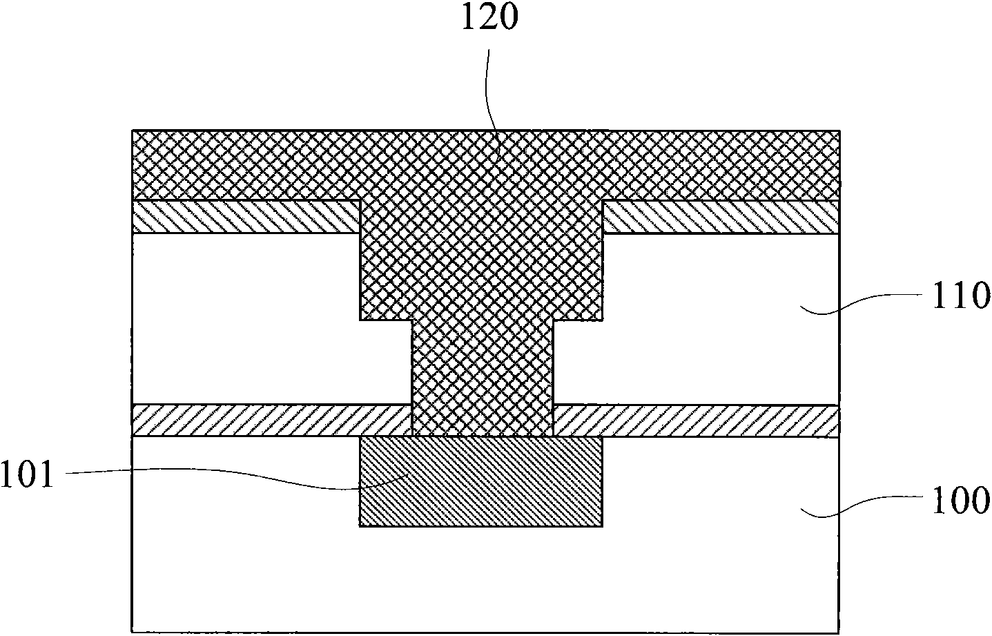
[0030] According to the background technology, when the chemical mechanical polishing process is used to remove the metal material on the low dielectric constant dielectric layer, a part of the thickness of the low dielectric constant dielectric layer will be damaged, resulting in the dielectric constant of the low dielectric constant dielectric layer Changes that affect the reliability of semiconductor devices. Therefore, the present invention provides a dual damascene structure and a manufacturing method thereof. In the manufacturing method of the dual damascene structure, after removing the metal material on the first low dielectric constant dielectric layer, the damaged first dielectric layer is removed, and the remaining A second low dielectric constant dielectric layer is formed on the first low dielectric constant dielectric layer to ensure that the dielectric constant value of the dielectric layer of the finally formed dual damascene structure is stable, and the first d...


PUM


Abstract

The invention discloses a dual-damascene structure and a manufacturing method thereof. The manufacturing method for the dual-damascene structure comprises the following steps: providing a semiconductor substrate, and forming a first low-dielectric constant dielectric layer on the semiconductor substrate and forming a trench and a through hole in the first low-dielectric constant dielectric layer; respectively forming metal materials on the first low-dielectric constant dielectric layer and in the trench and the through hole; removing the metal materials on the first low-dielectric constant dielectric layer by utilizing a chemical and mechanical lapping process, and forming a partially damaged first dielectric layer on the surface of the first low-dielectric constant dielectric layer by the chemical and mechanical lapping process; removing the damaged first dielectric layer; and forming a second low-dielectric constant dielectric layer on the remaining first low-dielectric constant dielectric layer. The dual-damascene structure disclosed by the invention can prevent the damaged first dielectric layer from generating adverse effects on the performances of subsequently formed metal interconnection lines and is beneficial to improving the reliability of semiconductor devices.

Description

technical field [0001] The invention relates to the field of integrated circuit manufacturing, in particular to a double damascene structure and a manufacturing method thereof. Background technique [0002] At present, the manufacturing technology of semiconductor devices is developing rapidly, semiconductor devices already have a deep submicron structure, and integrated circuits contain a huge number of semiconductor elements. With the further development of semiconductor device manufacturing technology, high-performance, high-density connections between semiconductor devices are not only performed in a single interconnection layer, but also interconnected between multiple layers. Therefore, a multilayer interconnection structure is generally provided in which a plurality of interconnection layers are stacked on top of each other with a dielectric layer interposed therebetween for connecting semiconductor devices. In particular, a multi-layer interconnection structure form...

Claims


Application Information

Patent Timeline
Patent Type & Authority Applications(China)
IPC IPC(8): H01L21/60H01L23/528
Inventor 张海洋周俊卿
Owner SEMICONDUCTOR MANUFACTURING INTERNATIONAL (BEIJING) CORP
Why Eureka
Try Eureka