Anti-sticking method for testing integrated circuit (IC) element and anti-sticking IC element test seat thereof

A component testing and component technology, applied in the direction of the measuring device shell, etc., can solve the problem of unobvious effect of the release type, and achieve the effect of simple structure, easy control and strong versatility

Active Publication Date: 2012-03-21
JIAXING JINGYAN INTELLIGENT EQUIP TECH
View PDF6 Cites 1 Cited by
  • Summary
  • Abstract
  • Description
  • Claims
  • Application Information

AI Technical Summary

Problems solved by technology

Although the designer has made various improvements to the lens mounting plate, such as opening air grooves on the lens mounting plate, roughen

Method used


Image

  • Anti-sticking method for testing integrated circuit (IC) element and anti-sticking IC element test seat thereof
  • Anti-sticking method for testing integrated circuit (IC) element and anti-sticking IC element test seat thereof
  • Anti-sticking method for testing integrated circuit (IC) element and anti-sticking IC element test seat thereof

Examples


Embodiment Construction

[0018] The present invention will be described in detail below through embodiments in conjunction with the accompanying drawings.

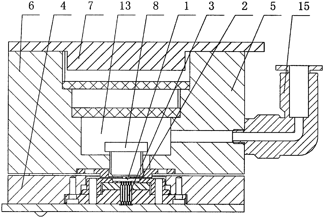
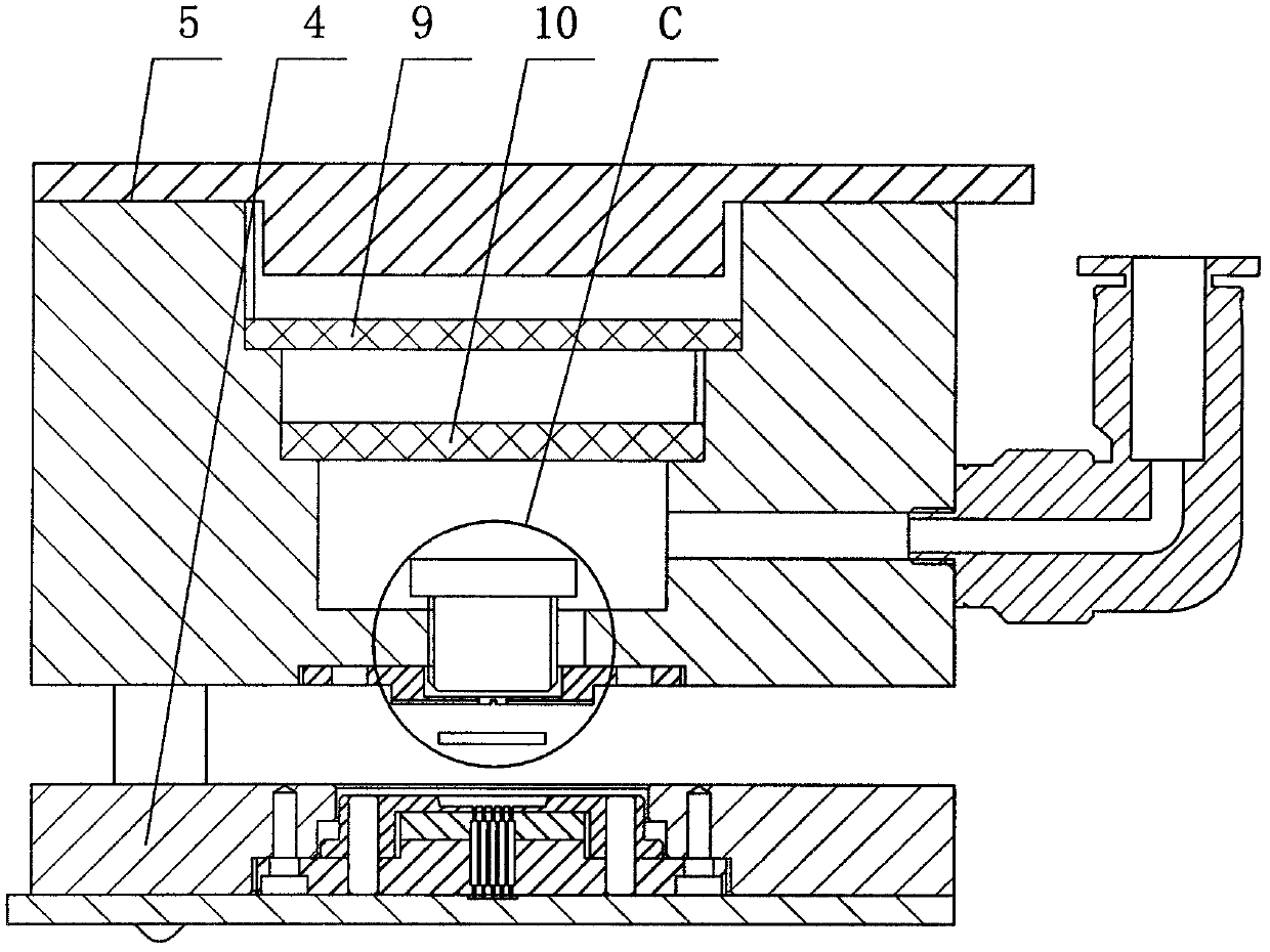
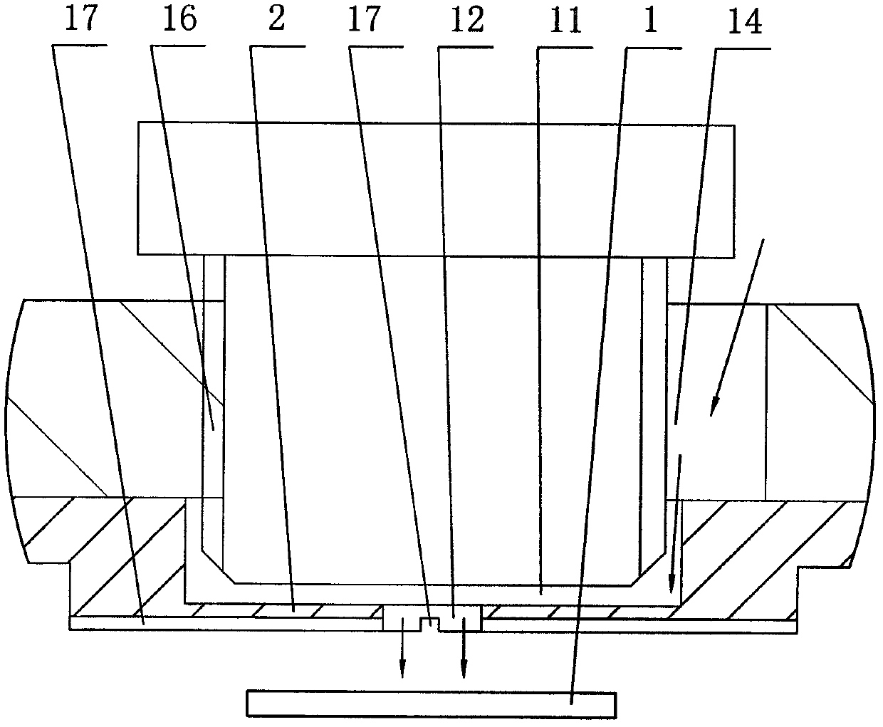
[0019] The technical solution adopted in the present invention is: introduce compressed air at the rear end of the contact surface of the IC component 1 and the upper mold, and use the compressed air to blow out the airflow between the contact surfaces of the upper mold to separate the contact surface of the IC component 1 and the upper mold. fall off. The contact surface of the upper mold is the lens mounting plate 2 .

[0020] figure 1 , figure 2 It is a structural schematic diagram of the anti-adhesive IC component 1 test seat manufactured by the anti-adhesive method for testing the IC component 1 . It includes a lower mold 4 for placing the tested IC component 1 and installing the test probe 3, and an upper mold 5 matched with the lower mold 4. The upper mold 5 includes an upper mold base 6, and the upper mold A light source PCB board 7 i...


PUM


Abstract

The invention relates to an anti-sticking method for testing an integrated circuit (IC) element and an anti-sticking IC element test seat thereof. The method is characterized in that: compressed air is introduced from a rear end of the IC element and an upper die contact surface, and the compressed air is used for blowing out the airflow between the contact surfaces of the upper die, so the IC element is separated from the contact surface of the upper die to drop off. The IC element test seat comprises a lower die and an upper die, wherein the lower die is used for holding the IC element to be tested and for installing a test probe, the upper die is combined with the lower die, the upper die comprises an upper die carrier, the rear end of the upper die carrier is provided with a light source printed circuit board (PCB), the front end of the upper die carrier is provided with a lens, a light equalizing plate is installed between the light source PCB and the lens, the upper die carrier on the front end of the lens is provided with a lens installation plate, the lens installation plate is the upper die contact surface of the IC element, the compressed air is led into a front cavity or a rear cavity which is formed between the upper die carrier and the front end of the lens and between the lens installation plate and the front end of the lens, and the lens installation plate on the position of the IC element contact surface is provided with a blowing hole, through which the front cavity is communicated with the atmosphere.

Description

technical field [0001] The invention relates to an anti-adhesive method for testing IC components and a device for testing the electrical parameter performance of IC components manufactured by the anti-adhesive method. Background technique [0002] In the past IC component testing process, there has always been a problem that after the test is over, when the upper mold of the test seat is lifted, the lens mounting plate of the upper mold will stick the IC component, which will cause the follow-up machine action to be unable to continue, resulting in a machine failure rate. High, reducing test efficiency. The reason is mainly two aspects: one is that during the process of pressing down the lens mounting plate, a negative pressure is generated between the small hole on the surface of the lens mounting plate and the IC component; the other is that the smooth surface of the lens mounting plate itself is in contact with the smooth surface of the IC component After that, vacuum a...

Claims


Application Information

Patent Timeline
IPC IPC(8): G01R1/04
Inventor 朱玉萍徐鹏辉
Owner JIAXING JINGYAN INTELLIGENT EQUIP TECH
Why Eureka
Try Eureka