
Patsnap Eureka
For R&D, Patsnap Eureka makes reading and utilizing patents & technical documents easy.
Patsnap Eureka AIR
Designed for self-driven R&D workflows. Generate viable solutions, solve complex R&D challenges, empower your innovation with AI.

Patsnap Eureka Materials
Designed for material experts only. Revolutionize your material R&D, from search, analyze, to developing new materials.

TechResearch
Generate reliable direction feasibility study reports for your R&D in just a few steps.

TechSeek
Discover and master advanced knowledge NOW. Basics, ideas, possibilities, all at once.

TechMind
As an expert in R&D Theories, TechMind can generates customized viable solutions instantly.

TechRisk
Analyze your overall solution with one click, know your potential R&D risks in advance.

TechMonitor
Get weekly tech updates, stay abreast of the latest tech innovations and key insights.
Fabrication of compact opto-electronic component packages
A technology of packages and components, applied in semiconductor/solid-state device manufacturing, electrical components, electrical solid-state devices, etc., can solve problems such as inflexible design changes, difficulties in specific application design, and large mechanical tolerances
- Summary
- Abstract
- Description
- Claims
- Application Information
AI Technical Summary
Problems solved by technology
Method used
Image

Examples
Embodiment Construction
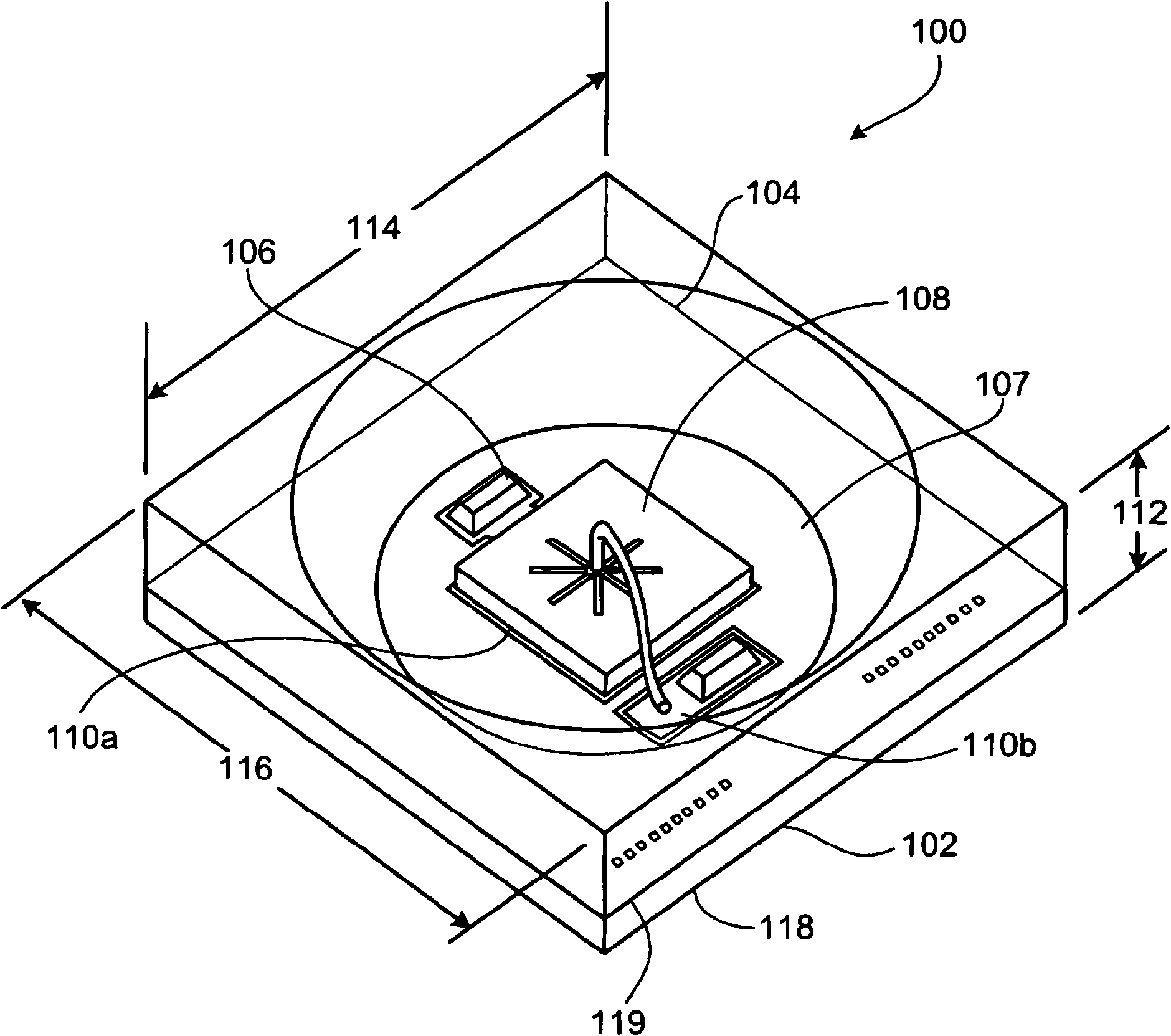
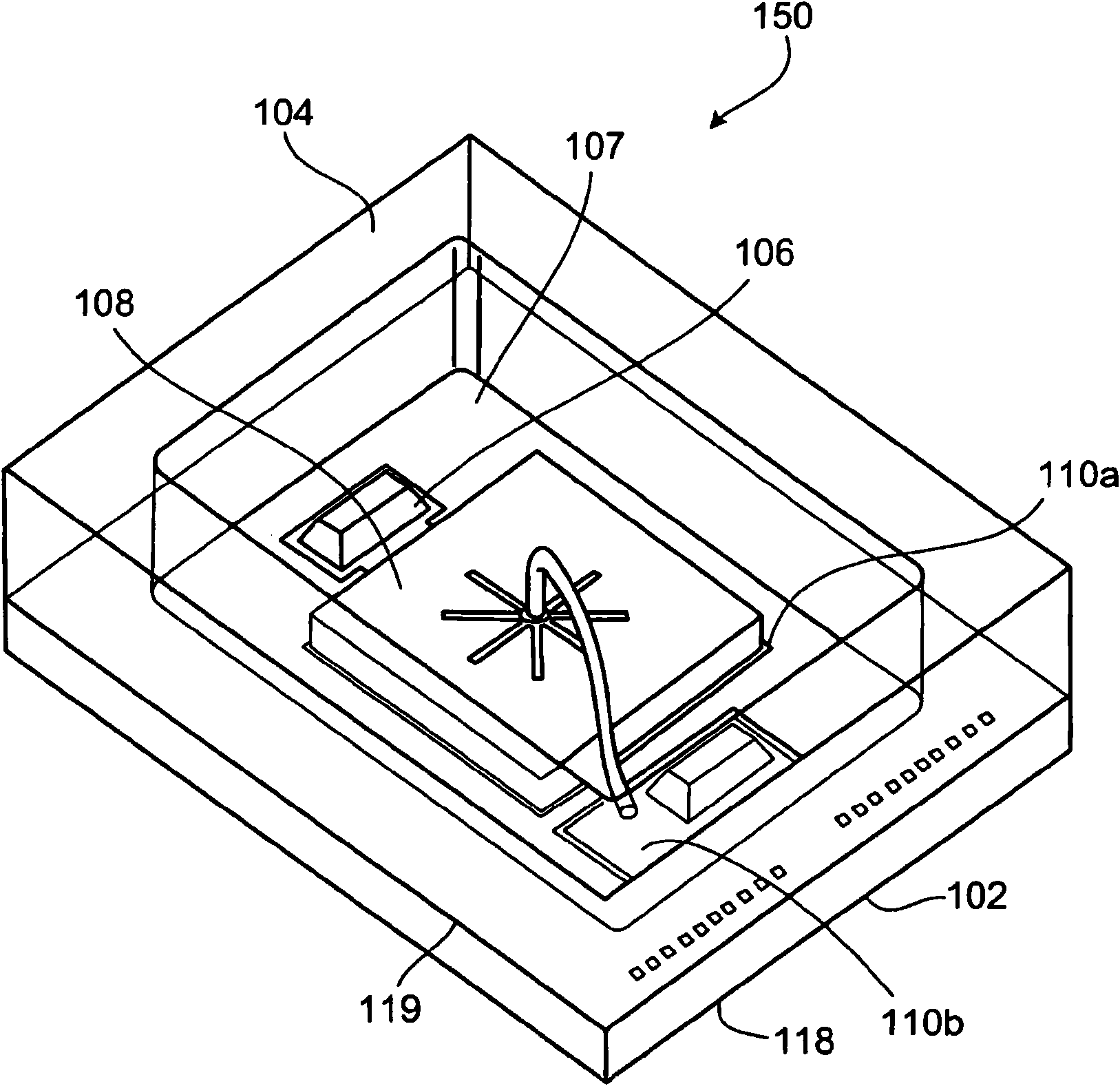
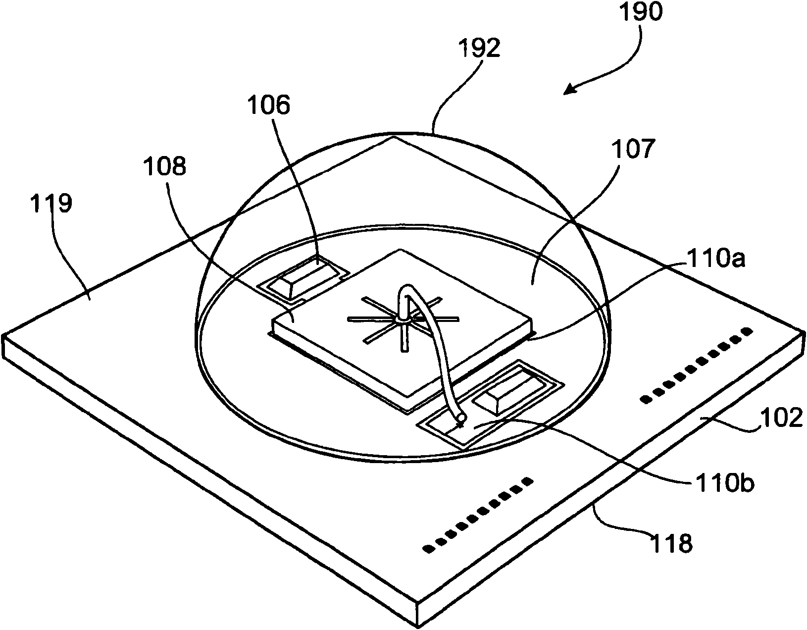
[0031] Figure 1a and Figure 1b Examples of thin LED packages 100 and 150 with enhanced thermal characteristics 100 and 150 are shown. Although Figure 1a and Figure 1b It is described relative to a light emitting diode 108, but the light emitting diode 108 can be replaced by other types of optoelectronic components. For example, in some applications, the LED 108 can be an infrared emitter (such as a vertical cavity surface emitting laser), an infrared receiver (such as a pin diode) or an infrared transceiver (infra-red transceiver). replace. Likewise, the manufacturing process described below can be used for the manufacture of encapsulations for optoelectronic components other than light-emitting diodes.
[0032] The LED package 100 includes a substrate 102, a reflector 104, a conductive metallization 106, a reflective surface 107, an LED 108, an LED die attach pad 110a (located below the LED 108) and The wire bonding pads 110b. In the illustrated example, substrate 10...
PUM
 Abstract
Description
Claims
Application Information
 - R&D Engineer
- R&D Manager
- IP Professional
- Industry Leading Data Capabilities
- Powerful AI technology
- Patent DNA Extraction
Browse by: Latest US Patents, China's latest patents, Technical Efficacy Thesaurus, Application Domain, Technology Topic, Popular Technical Reports.
© 2024 PatSnap. All rights reserved.Legal|Privacy policy|Modern Slavery Act Transparency Statement|Sitemap|About US| Contact US: help@patsnap.com