Wafer Bow Measurement Method

A technology of curvature and wafer thickness, applied in the field of wafer curvature measurement

Active Publication Date: 2016-06-22
SHANGHAI HUAHONG GRACE SEMICON MFG CORP
View PDF4 Cites 0 Cited by
  • Summary
  • Abstract
  • Description
  • Claims
  • Application Information

AI Technical Summary

Problems solved by technology

[0003] Since WaferBow is directly related to wafer performance, the industry provides a variety of WaferBow calculation methods, but these calculation methods can only be used to calculate WaferBow after thinning is completed. The WaferBow solution to avoid the WaferBow being too large after the thinning process is completed

Method used


Image

  • Wafer Bow Measurement Method

Examples


Embodiment Construction

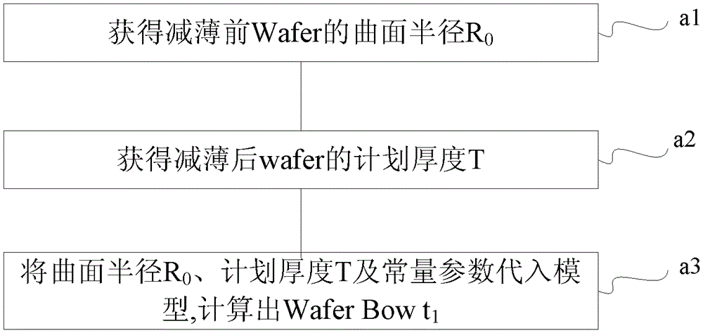
[0011] Combine below figure 1 A specific implementation is given.

[0012] Step a1, obtain the surface radius R of the Wafer before thinning 0 , the surface radius R 0 It can be directly measured and obtained by the film stress measuring machine.

[0013] In step a2, the planned thickness T of the thinned wafer is obtained, which is the thickness of the thinned wafer set by the process and is related to the specific process.

[0014] Step a3, the surface radius R 0 , planned thickness T and constant parameters are substituted into the model, [R 0 T 2 -(R 0 2 T 4 -r 2 T 0 4 ) 1 / 2 ] / T 0 2 +C(T 0 / T) 1.58 Calculate WaferBowt 1 , where T 0 In order to reduce the thickness of the wafer, r is the radius of the wafer, and C is the curvature of the wafer caused by the gravity of the wafer before thinning. For a wafer of a specific size, its value is a constant, for example, for an 8-inch wafer, C is about 0.11, and there are corresponding C values ​​for 6-inch and 1...


PUM


Abstract

The invention provides a Wafer Bow calculation method to measure and calculate the Wafer Bow before the thinning process, so as to avoid various losses caused by discovering that the Wafer Bow does not meet the requirements after the thinning process is completed. A method for calculating Wafer Bow provided by the present invention comprises the steps of: obtaining the curved surface radius R of the Wafer before thinning 0 and the planned thickness T of the wafer after thinning; according to the surface radius R 0 and the planned thickness T, calculate the Wafer Bow of the thinned wafer as t 1 , the model used in this calculation is: t 1 =[R 0 T 2 -(R 0 2 T 4 -r 2 T 0 4 ) 1 / 2 ] / T 0 2 +C( T 0 / T) 1.58 , where T 0 For the wafer thickness before thinning, r is the radius of the wafer, and C is the curvature of the wafer caused by the gravity of the wafer before thinning.

Description

technical field [0001] The invention relates to the field of integrated circuit manufacturing, in particular to a wafer bow (WaferBow) measurement method. Background technique [0002] In the integrated circuit manufacturing process, wafers are often subjected to thinning processes, such as chemical mechanical grinding processes, etc., but in the wafer thinning process, it often occurs that the closer to the center of the wafer, the greater the thinning thickness, and the formation of wafer surface The phenomenon of concave shallow bowl shape, which has a negative impact on the wafer. The industry generally uses the parameter WaferBow to evaluate the concave degree, and the WaferBow refers to the vertical distance between the highest point and the lowest point on the wafer surface after thinning. [0003] Since WaferBow is directly related to wafer performance, the industry provides a variety of WaferBow calculation methods, but these calculation methods can only be used to...

Claims


Application Information

Patent Timeline
Patent Type & Authority Patents(China)
IPC IPC(8): H01L21/66G01B21/20
Inventor 傅荣颢刘玮荪
Owner SHANGHAI HUAHONG GRACE SEMICON MFG CORP
Why Eureka
Try Eureka