

Method of manufacturing circuit pattern through sputtering technology and rewiring method of chip
A technology of circuit pattern and sputtering process, applied in circuits, semiconductor/solid-state device manufacturing, electrical components, etc., can solve the problems of many steps and complex processes, and achieve the effect of reducing etching steps, shortening the process flow, and reducing the difficulty of the process
- Summary
- Abstract
- Description
- Claims
- Application Information
AI Technical Summary
Problems solved by technology
Method used
Image

Examples
Embodiment 1
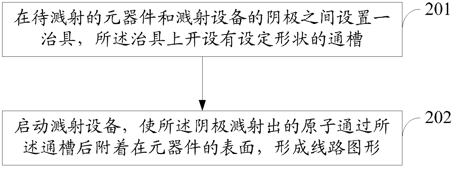
[0028] Please refer to figure 1 , an embodiment of the present invention provides a method for making a circuit pattern through a sputtering process, including:
[0029] 201. A jig is set between the component to be sputtered and the cathode of the sputtering equipment, and a through groove of a predetermined shape is opened on the jig.
[0030] The existing sputtering method is generally to sputter the entire surface of the components to be sputtered, such as circuit boards or chips, that is, place the components in the sputtering chamber of the sputtering equipment, start the sputtering equipment, The atoms sputtered by the cathode of the sputtering equipment act on the entire surface of the component without any shielding, forming a layer of sputtering layer on the entire surface of the component. Subsequently, etching and other methods are used to remove the sputtered layer in unnecessary parts, and only retain the sputtered layer in required parts, thereby forming a circ...
Embodiment 2
[0039] Please refer to Figure 4 , an embodiment of the present invention provides a chip rewiring method, including:
[0040] 301. Set a photoresist on the surface of the chip, where the photoresist covers areas on the chip other than original pads.
[0041] Such as Figure 5a As shown, a layer of photoresist 460 can be completely coated on the surface of the chip 440, and then, through exposure and development processes, the photoresist 460 on the original pads 450 that need RDL on the chip is removed, so that these original pads 450 exposed, while other parts on the chip 440 are still covered by the photoresist 460 .
[0042] 302. Use the method described in Embodiment 1 to sputter the chip to form a required circuit pattern.
[0043] Such as Figure 5b As shown, in this step, the method for making circuit patterns by the sputtering process described in Embodiment 1 is used to sputter the chip 440, and the chip 440 is directly sputtered on the surface of the chip 440 by...
PUM
 Abstract
Description
Claims
Application Information