
Data error check method, data transfer method, and semiconductor memory

A technology of error checking and storage devices, applied in the direction of error detection/correction, static memory, electrical digital data processing, etc., can solve the problems of six-level gate delay, increase of circuit area and error checking time, increase of circuit area, etc.

Active Publication Date: 2012-05-23
SK HYNIX INC
View PDF5 Cites 6 Cited by
  • Summary
  • Abstract
  • Description
  • Claims
  • Application Information

AI Technical Summary

Problems solved by technology

[0008] To configure this CRC logic, a total of 328 2-input XOR gates and 42 polynomial equations are required, resulting in an increase in circuit area
[0009] In addition, the final CRC value is calculated by passing through the six-level XOR gate path, resulting in a six-level gate delay
[0010] One problem with typical semiconductor circuits according to the prior art is that the circuit area and error checking time increase due to the equations required by the CRC logic

Method used


Image

  • Data error check method, data transfer method, and semiconductor memory
  • Data error check method, data transfer method, and semiconductor memory
  • Data error check method, data transfer method, and semiconductor memory

Examples


Embodiment Construction

[0024] Reference will now be made in detail to exemplary embodiments according to the present invention and examples illustrated in the accompanying drawings. Wherever possible, the same reference numbers will be used throughout the drawings to refer to the same or like parts.

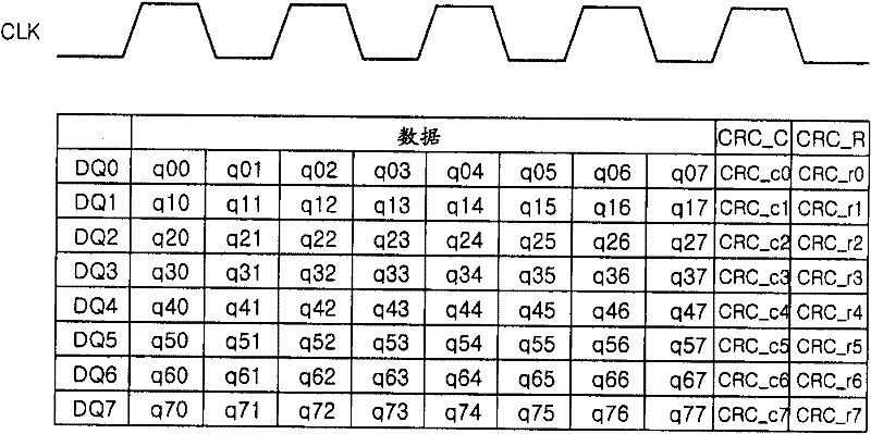
[0025] According to an exemplary embodiment, the first error check in the column direction and the second error check in the row direction are performed on the data transferred through the data input / output terminals DQ0 to DQ7 to generate corresponding error check signals, and are transmitted via the data bus Send the error check signal to the outside.

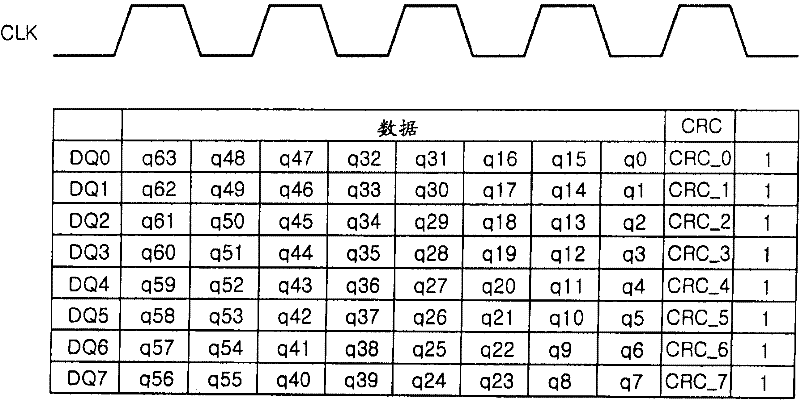
[0026] Typically, a unit time interval is allocated for error checking signals. That is, if figure 1 As shown, five clock signals CLK are used in order to transmit 8-bit data and 1-bit error check signal. Therefore, since two unit time intervals are allocated to one clock signal, the tenth unit time interval is redundant in typical practice.

[00...


PUM


Abstract

Various embodiments of a memory system are disclosed. In one exemplary embodiment, the memory system may include a semiconductor memory apparatus configured to generate error check signals in a column direction and a row direction of data groups to be transmitted through a plurality of data input / output terminals in a read operation and output the error check signals together with the data groups, and a memory controller configured to control data read / write operations of the semiconductor memory apparatus, generate error check signals by performing error check in a column direction and a row direction of data groups to be transmitted in a write operation, and provide the error check signals to the semiconductor memory apparatus together with the data groups.

Description

[0001] Cross References to Related Applications [0002] This application claims priority from Korean Patent Application No. 10-2010-0106861 filed with the Korean Intellectual Property Office on Oct. 29, 2010, the entire contents of which are incorporated herein by reference. technical field [0003] The present invention relates generally to data error checking, and more particularly to a data error checking circuit, a data error checking method, a data transmission method using a data error checking function, a semiconductor memory device and a storage system using a data error checking function. Background technique [0004] A typical semiconductor circuit may have an error check function for checking whether an error has occurred in data in order to improve data reliability of high-speed data transmission. A typical error checking method is a cyclic redundancy check (CRC, cyclic redundancy check) function. [0005] figure 1 is a diagram of a typical semiconductor circu...

Claims


Application Information

Patent Timeline
Patent Type & Authority Applications(China)
IPC IPC(8): G11C29/44
CPCG06F11/1004G11C2029/0411
Inventor 李仲缟
Owner SK HYNIX INC
Features
  • Generate Ideas
  • Intellectual Property
  • Life Sciences
  • Materials
  • Tech Scout
  • Unparalleled Data Quality
  • Higher Quality Content
  • 60% Fewer Hallucinations
Learn More