Method for manufacturing circuit boards
A manufacturing method and circuit board technology, which are applied in the directions of printed circuit manufacturing, printed circuits, electrical components, etc., can solve problems such as unfavorable circuit board quality, separation of adhesive layers, and high stress on the connection part of flexible printed circuit boards.
Active Publication Date: 2012-05-30
AVARY HLDG (SHENZHEN) CO LTD +1
4 Cites 8 Cited by
AI-Extracted Technical Summary
Problems solved by technology
The connection part of the flexible printed circuit board has relatively high stress and is easy to s...
Abstract
A method for manufacturing circuit boards includes steps of providing a flexible circuit board which is provided with a first connecting area, a second connecting area and a blank area, manufacturing at least one opening or a plurality of through holes in the blank area, applying adhesive in the first connecting area, and bending the flexible circuit board along the extending direction of the openings or the through holes so as to lead the second connecting area to be adhered to the first connecting area through adhesives, wherein the blank area is connected between the first connecting area and the second connecting area, and conductive circuits are distributed in at least one of the first connecting area and the second connecting area.
Application Domain
Printed circuit manufacture
Technology Topic
AdhesiveEngineering +1
Image
Examples
- Experimental program(1)
Example Embodiment
[0039] The manufacturing method of the circuit board provided by the technical solution will be described in further detail below in conjunction with the accompanying drawings and multiple embodiments.
[0040] The first embodiment of the technical solution provides a method for manufacturing a circuit board, which includes the following steps:
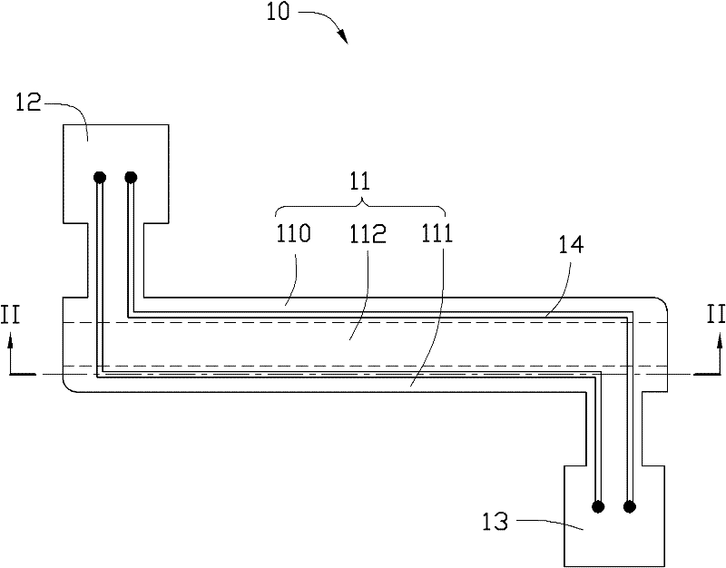
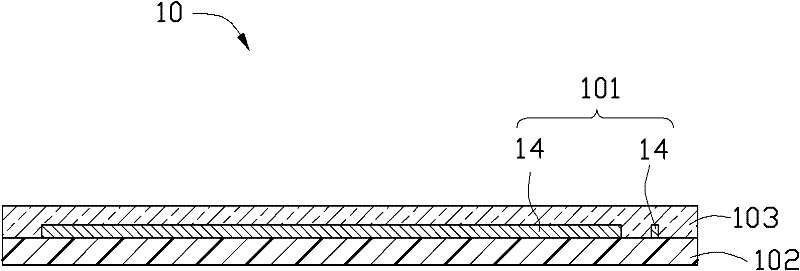
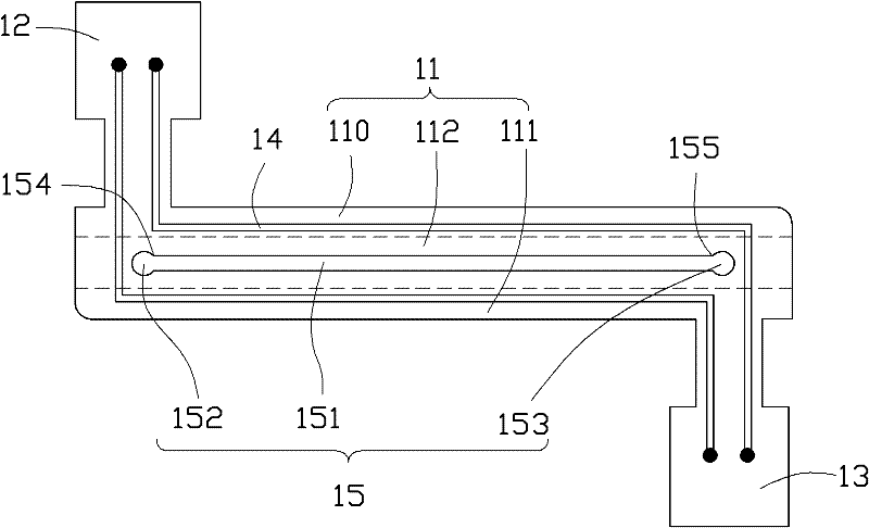
[0041] The first step, please refer to figure 1 with figure 2 , Provide a flexible circuit board 10, which includes a connecting portion 11, a first flexible substrate portion 12 and a second flexible substrate portion 13. The connecting portion 11 has a rectangular parallelepiped shape. The connection portion 11 includes a first connection area 110, a second connection area 111 and a blank area 112 connected between the first connection area 110 and the second connection area 111. At least one of the first connection area 110 and the second connection area 111 has a conductive circuit 14 distributed therein. The conductive line 14 is used for signal connection between the first flexible substrate portion 12 and the second flexible substrate portion 13. In this embodiment, the number of conductive lines 14 is two. One conductive line 14 is located in the first connection area 110 and is close to a side of the connection portion 11, and the other conductive line 14 is located in the second connection area. Area 111, and close to the other side of the connecting portion 11. In this embodiment, each conductive circuit 14 is a straight line. Of course, the conductive circuit 14 is not limited to a straight line, and may also be a broken line or a curve. The first flexible substrate portion 12 and the second flexible substrate portion 13 are respectively connected to opposite ends of the connecting portion 11. Specifically, the first flexible substrate portion 12 is connected to one end of the first connection area 110 away from the blank area 112, and the second flexible substrate portion 13 is connected to the other end of the second connection area 111 away from the blank area 112.
[0042] The flexible circuit board 10 can be a double-sided copper-clad base film or a multilayer flexible circuit board. See figure 2 In this embodiment, the flexible circuit board 10 is a single-sided copper-clad base film with conductive patterns formed. The flexible circuit board 10 includes a conductive circuit layer 101 and an insulating layer 102 stacked on each other, and a cover film 103 for protecting the conductive circuit. The conductive circuit layer 101 may be a patterned copper layer. The plurality of conductive circuits 14 are located on the conductive circuit layer 101. The insulating layer 102 is a polyester (PET) film or a polyimide (PI) film.
[0043] The second step, please refer to figure 1 with image 3 , An opening 15 is formed in the blank area 112. The opening 15 can be formed by punching or laser cutting. In this embodiment, the opening 15 is arranged along the length direction of the connecting portion 11 and includes a first end hole 152, a through groove 151 and a second end hole 153 that are connected in sequence. The through groove 151 is elongated and has a first end 154 and a second end 155 opposite to each other. The first end 154 is close to the first flexible substrate section 12, and the second end 155 is close to the second end. The flexible substrate portion 13. The cross sections of the first end hole 152 and the second end hole 153 are both circular, the first end hole 152 is close to the first end 154, and the second end hole 153 is close to the second end 155. The apertures of the first end hole 152 and the second end hole 153 are both larger than the width of the through groove 151. In this way, the first end hole 152 and the second end hole 153 can reduce the stress at the end of the through groove 151 and prevent the connecting portion 11 from cracking from the opening 15.
[0044] The third step, please refer to Figure 4 , The adhesive 16 is coated on the first connection area 110. An adhesive 16 is provided, and the adhesive 16 is applied to the first connection area 110 to obtain Figure 4 The structure shown. The adhesive 16 may be a fast thermal curing adhesive, which includes epoxy resin, polymethyl methacrylate or a mixture thereof. During bonding, the rapid thermal curing adhesive can be chemically bonded, which can produce greater bonding strength. In this embodiment, the adhesive 16 is coated on the side of the first connection area 110 close to the insulating layer 102.
[0045] The fourth step, please refer to Figure 5 with Image 6 The flexible circuit board 10 is bent along the extending direction of the at least one opening 15 so that the second connection area 111 is bonded to the first connection area 110 by the adhesive 16. Specifically, the following steps can be taken:
[0046] First, the flexible circuit board 10 is bent along the extending direction of the at least one opening 15 to attach the second connection area 111 to the first connection area 110. When the second connection area 111 is attached to the first connection area 110, the connection portion 11 can be heated and pressurized. In this embodiment, when the second connection area 111 is attached to the first connection area 110, the temperature range of the connection portion 11 is 60 degrees Celsius to 100 degrees Celsius, and the pressure range is 0.1 MPa to 0.3 MPa. .
[0047] Then, the flexible circuit board 10 is pressed so that the adhesive 16 is filled between the second connection area 111 and the first connection area 110, and is also filled in the at least one opening 15 to obtain Figure 5 with Image 6 The structure shown. The temperature and pressure of the connecting portion 11 when the second connecting area 111 is pressed to the first connecting area 110 are higher than when the second connecting area 111 is pressed to the first connecting area 110 The temperature and pressure of the connecting portion 11. In this embodiment, when the second connection area 111 is pressed to the first connection area 110, the temperature range of the connection portion 11 is 100 degrees Celsius to 150 degrees Celsius, and the pressure range is 0.3 MPa to 0.7 MPa. . During the pressing process, the adhesive 16 flows between the second connection area 111 and the first connection area 110 and fills the opening 15 to obtain the circuit board 100.
[0048] Of course, before the adhesive 16 is applied to the first connection area 110, one or more hard circuit boards may be provided, and the hard circuit boards are pressed and connected to the first flexible substrate portion 12 and/or the second flexible substrate portion 13, so that a rigid-flex circuit board can be obtained.
[0049] The manufacturing method of the circuit board provided by the first embodiment of the technical solution forms an opening 15 in the connecting portion 11, which can reduce the stress of the connecting portion 11 when bending along the opening 15 and avoid the connecting portion 11 and the adhesive 16 Separation between. In addition, the formed adhesive 16 is filled in the opening 15 to further increase the bonding strength between the connecting portion 11 and the adhesive 16, which is beneficial to improve the quality of the manufactured circuit board 100.
[0050] See Figure 7 , The manufacturing method of the circuit board provided by the second embodiment of the technical solution includes the steps:
[0051] The first step is roughly the same as the first embodiment, with the difference that the connecting portion 21 of the provided flexible circuit board 20 is roughly rectangular parallelepiped, and its two sides are slightly outward near the first flexible substrate portion 22 Protruding. Correspondingly, the two conductive lines 24 also slightly protrude outward near the first flexible substrate portion 22.
[0052] In the second step, the difference from the first embodiment is that two openings extending substantially along the folding direction of the connecting portion 21, that is, the length direction of the connecting portion 21, are formed, where the first opening 250 is close to the first flexible substrate The second opening 26 is close to the second flexible substrate portion 23. The first opening 250 includes a first end hole 252, a through groove 251, and a second end hole 253 that are connected in sequence. The through groove 251 also has a first end 254 close to the first flexible substrate portion 22 and a second end 255 close to the second flexible substrate portion 23. Corresponding to the shape of the edge of the connecting portion 21 and the shape of the conductive circuit 24, the edge of the through slot 251 of the first opening 250 also protrudes outward at the center thereof. The first end hole 252 is close to the first end 254, and the second end hole 253 is close to the second end 255. The apertures of the first end hole 252 and the second end hole 253 are both larger than the width of the through groove 251. Similar to the first opening 250, the second opening 26 also includes a first end hole (not shown in the figure), a through slot (not shown) and a second end hole (not shown in the figure) that are connected in sequence. The apertures of the first end hole and the second end hole are both larger than the width of the through groove. The through groove of the second opening 26 also has a first end close to the first flexible substrate portion 22 and a second end close to the second flexible substrate portion 23. The second end (not shown) of the through slot of the second opening 26 is adjacent to the first end 254 of the first opening 250. Different from the first opening 250, the through groove of the second opening 26 is elongated.
[0053] The third step and the fourth step are roughly the same as those of the first embodiment. An adhesive (not shown) can be applied to the first connection area (not shown). Then, the flexible circuit board 20 is bent along the extending direction of the first opening 250 and the second opening 26, and the second connection area (not shown) is attached to the first connection area. Finally, the flexible circuit board 20 is pressed so that the adhesive is filled between the second connection area and the first connection area, and is also filled in the first opening 250 and the second opening 26 respectively.
[0054] Of course, the edge of the connecting portion 21 and the shape of the conductive circuit 24 are not limited to protruding outward near the first flexible substrate portion 22, and there may be many variations.
[0055] Among the two openings formed by the manufacturing method of the circuit board of the second embodiment of the technical solution, the first opening 250 has an edge shape corresponding to the outer shape of the connecting portion 21, which can more effectively distribute the stress in the connecting portion 21. Homogenization to avoid separation between the connecting portion 21 and the adhesive (not shown).
[0056] See Figure 8 , The third embodiment of the present technical solution provides a manufacturing method of a circuit board, including the steps:
[0057] The first step is roughly the same as that of the first embodiment. The provided connection part 31 of the flexible circuit board 30 also includes a first connection area 310, a second connection area 311, and is connected to the first connection area 310 and the second connection area. The blank area 312 between 311. The two conductive lines 34 both extend substantially along the length direction of the connecting portion 31.
[0058] In the second step, different from the first embodiment, a plurality of through holes 35 are formed in the blank area 312, and the plurality of through holes 35 extend substantially along the folding direction of the connecting portion 31. In this embodiment, the folding direction of the connecting portion 31 is the length direction of the connecting portion 31, in other words, it is substantially the same as the extending direction of the conductive circuit 34.
[0059] The third step and the fourth step are roughly the same as those of the first embodiment. An adhesive (not shown) can be applied to the first connection area (not shown). Then, the flexible circuit board 30 is bent along the extending direction of the plurality of sequentially arranged through holes 35, and the second connection area (not shown) is attached to the first connection area. Finally, the flexible circuit board 30 is pressed to make the adhesive fill between the second connection area and the first connection area, and also fill the plurality of through holes 35.
[0060] Of course, before the adhesive is applied to the first connection area, one or more rigid circuit boards can also be provided, and the rigid circuit boards are pressed and connected to the first flexible substrate portion (Figure (Not shown) and/or the second flexible substrate portion (not shown), so as to obtain a rigid-flex circuit board.
[0061] The method for manufacturing the circuit board of the third embodiment of the present technical solution forms a plurality of through holes 35 arranged in sequence, which can prevent the connection portion 31 from being separated from the adhesive and at the same time prevent the connection portion 31 from cracking.
[0062] It is understandable that for those of ordinary skill in the art, various other corresponding changes and modifications can be made according to the technical concept of the present invention, and all these changes and modifications should fall within the protection scope of the claims of the present invention.
PUM


Description & Claims & Application Information
We can also present the details of the Description, Claims and Application information to help users get a comprehensive understanding of the technical details of the patent, such as background art, summary of invention, brief description of drawings, description of embodiments, and other original content. On the other hand, users can also determine the specific scope of protection of the technology through the list of claims; as well as understand the changes in the life cycle of the technology with the presentation of the patent timeline. Login to view more.