Array substrate, preparation method thereof and electric paper display
An array substrate and manufacturing method technology, applied in the field of active display, can solve the problems of poor feasibility and high requirements, and achieve the effects of reducing influence, simplifying manufacturing process, and saving manufacturing cost
- Summary
- Abstract
- Description
- Claims
- Application Information
AI Technical Summary
Problems solved by technology
Method used
Image

Examples
Embodiment 1
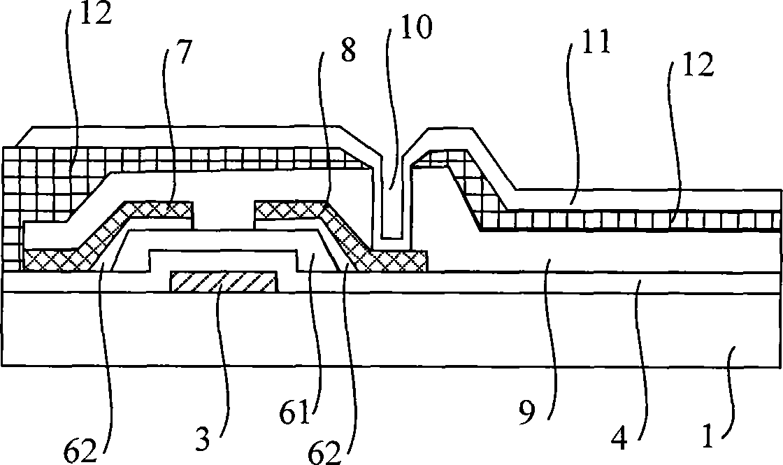
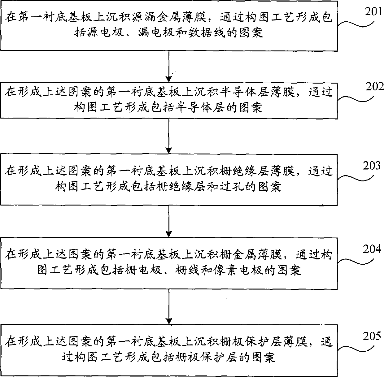
[0042] figure 2 A flow chart of the method for manufacturing an array substrate provided in Embodiment 1 of the present invention, as shown in figure 2 As shown, the manufacturing method of the array substrate includes:
[0043] Step 201, depositing a source-drain metal thin film on the first substrate, and forming a pattern including source electrodes, drain electrodes and data lines through a patterning process;
[0044]Specifically, a sputtering process can be used to deposit a source-drain metal film on the first base substrate, wherein the source-drain metal film can use metal elements such as aluminum (Al), molybdenum (Mo), and neodymium (Nd); then, by The patterning process forms patterns such as source electrodes, drain electrodes, and data lines. Wherein, the region between the source electrode and the drain electrode is a TFT channel.
[0045] Step 202, depositing a semiconductor layer thin film on the first base substrate with the above pattern formed, and form...
Embodiment 2
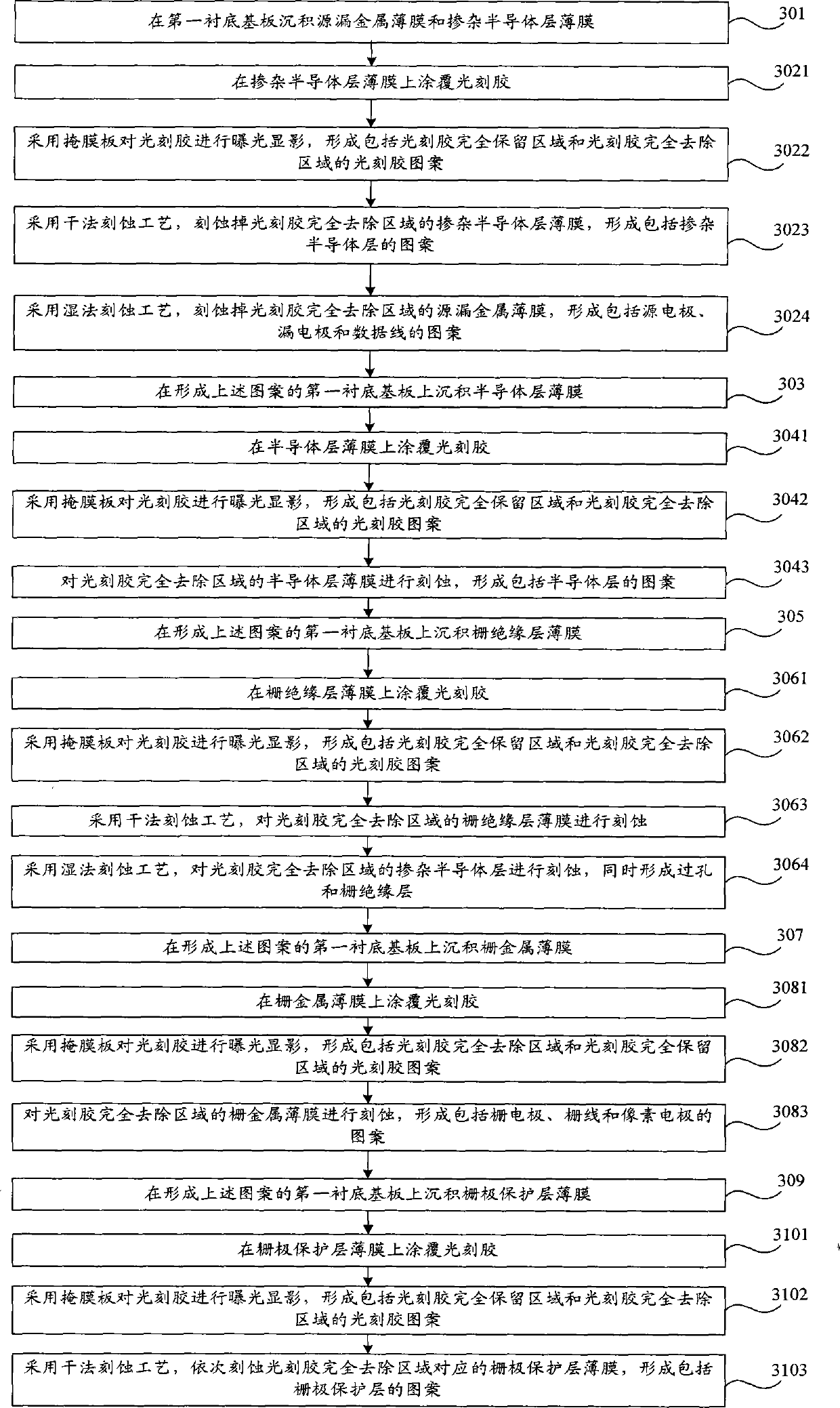
[0055] Figure 3A The flow chart of the manufacturing method of the array substrate provided in Embodiment 2 of the present invention, on the basis of Embodiment 1, the array substrate formed by the manufacturing method of the array substrate can be used in a reflective active display (such as an electronic paper display) The main difference is that, in this embodiment, a doped semiconductor layer is included above the source electrode, the drain electrode and the data line. Such as Figure 3A As shown, the manufacturing method of the present embodiment includes:
[0056] Step 301, depositing a source-drain metal thin film and a doped semiconductor layer thin film on the first base substrate; specifically, the source-drain metal thin film can be deposited on the first base substrate by a sputtering process, and then the source-drain metal film can be deposited on the source-drain metal film by PECVD. A doped semiconductor layer film is deposited on the film. Wherein, the ma...
Embodiment 3
[0090] Figure 4A The flow chart of the manufacturing method of the array substrate provided by the third embodiment of the present invention, this embodiment can be realized based on the first or second embodiment, taking the second embodiment as an example, the difference is that this embodiment includes While doping the pattern of the semiconductor layer, the source electrode, the drain electrode and the data line, it also includes: forming a storage capacitor. Such as Figure 4A As shown, the steps of forming a pattern comprising a doped semiconductor layer, a source electrode, a drain electrode, a data line and a storage capacitor include:
[0091] Step 2011, coating photoresist on the doped semiconductor layer thin film;
[0092] Step 2012, using a mask to expose and develop the photoresist to form a photoresist pattern including a photoresist completely reserved area and a photoresist completely removed area;
[0093] Step 2013, using a dry etching process to etch aw...
PUM
 Abstract
Description
Claims
Application Information
 - R&D Engineer
- R&D Manager
- IP Professional
- Industry Leading Data Capabilities
- Powerful AI technology
- Patent DNA Extraction
Browse by: Latest US Patents, China's latest patents, Technical Efficacy Thesaurus, Application Domain, Technology Topic.
© 2024 PatSnap. All rights reserved.Legal|Privacy policy|Modern Slavery Act Transparency Statement|Sitemap