Method for manufacturing T-shaped gate by adopting single electron beam exposure

A technology of electron beam exposure and electron beam glue, which is applied in the field of preparing T-shaped grids by single electron beam exposure, can solve the problems of alignment error, high time and cost, and high cost per unit time of two exposures, and achieve a reduction in machine Occupying cost and reducing writing area

Active Publication Date: 2014-01-08
INST OF MICROELECTRONICS CHINESE ACAD OF SCI
View PDF5 Cites 0 Cited by
  • Summary
  • Abstract
  • Description
  • Claims
  • Application Information

AI Technical Summary

Problems solved by technology

[0004] In order to achieve the size of the T-shaped grid, electron beam exposure technology is usually used. Those skilled in the art know that electron beam exposure writes graphics point by point, and the time spent is proportional to the total writing area, and its unit time higher cost
For example, since the size of the grid cap is usually several times that of the grid pin, if the electron beam exposure is performed on the grid cap and the grid pin pattern separately, the time and cost required are much higher, and it is possible to expose the grid cap and the grid pin separately. Problems with misalignment of two exposures, resulting in poor gate topography

Method used


Image

  • Method for manufacturing T-shaped gate by adopting single electron beam exposure
  • Method for manufacturing T-shaped gate by adopting single electron beam exposure
  • Method for manufacturing T-shaped gate by adopting single electron beam exposure

Examples


Embodiment Construction

[0023] In order to make the object, technical solution and advantages of the present invention clearer, the present invention will be further described in detail below in conjunction with specific embodiments and with reference to the accompanying drawings.

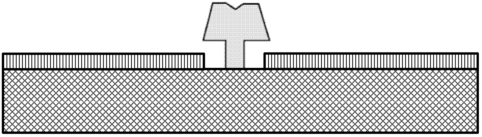
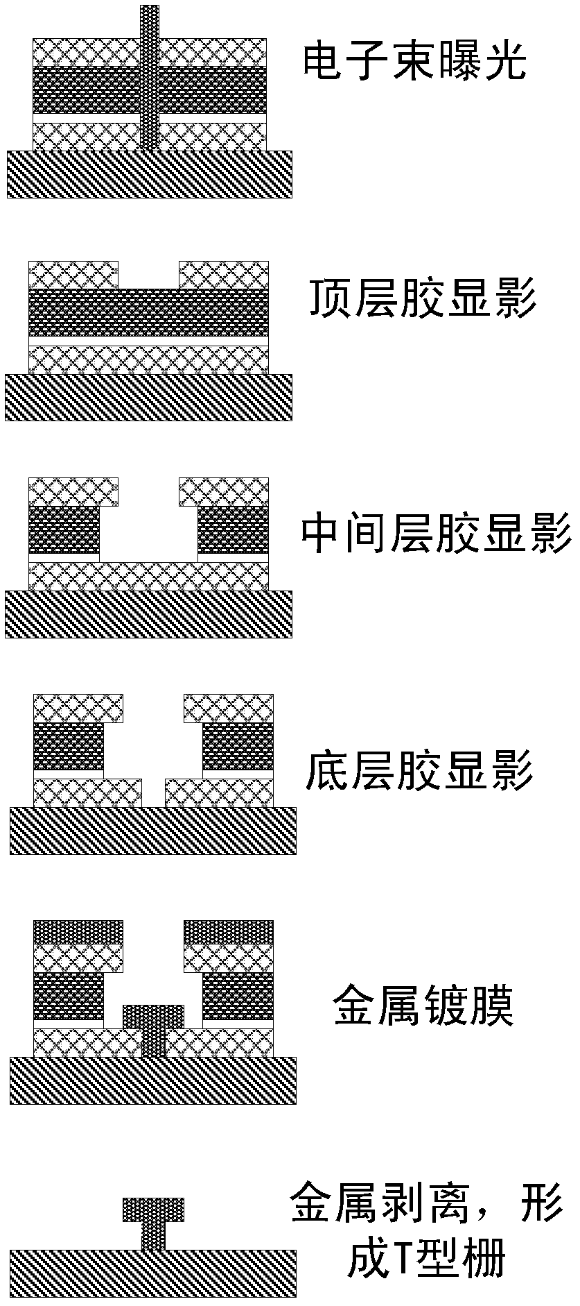
[0024] The method for preparing a T-shaped grid by using a single electron beam exposure provided by the present invention adopts a four-layer laminated glue, only needs to expose the grid pin pattern once, and through multiple layers of development, the grid cap and grid cap can be formed. Graphics required for grid pins.

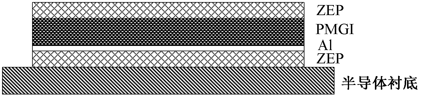
[0025] The lamination glue structure that the present invention adopts is as figure 2 As shown, it is divided into 4 layers from bottom to top, which are the bottom electron beam glue ZEP, metal aluminum (Al), electron beam glue PMGI and the top electron beam glue ZEP, among which:

[0026] The bottom electron beam glue ZEP is formed on the semiconductor substrate, and its thickness is selected to b...


PUM

PropertyMeasurementUnit
thicknessaaaaaaaaaa
thicknessaaaaaaaaaa
sizeaaaaaaaaaa

Abstract

The invention discloses a method for manufacturing a T-shaped gate by adopting single electron beam exposure. The method comprises the following steps of: performing electron beam exposure on laminated resist on a substrate to write a gate pin pattern; developing the laminated resist, forming a gate pin pattern and a gate cover pattern of the laminated resist by utilizing different characteristics of each layer of resist; and performing metal film plating and stripping on the substrate with the gate pin pattern and gate cover pattern of the laminated resist to form the T-shaped gate. The four-layer laminated resist with high stability is adopted, and a space pattern required by the T-shaped gate can be obtained by performing the single electron beam exposure to write the gate pin pattern and combining a multiple layering development method to manufacture the T-shaped gate. By the method, the writing area of an electron beam is effectively reduced, and occupied machines and hours are reduced correspondingly.

Description

technical field [0001] The invention relates to the technical field of semiconductor devices, in particular to a method for preparing a T-shaped grid by single electron beam exposure. Background technique [0002] The gate preparation of field effect devices is one of the most important process links. According to the size effect of the device, reducing the gate length is an important means to improve the high frequency performance of the device. Reducing the gate length requires a thinner gate line manufacturing process, but if the gate line is too thin, its parasitic resistance will increase, which is not conducive to high-gain and high-power applications. Therefore, for commonly used high-gain or high-power For power devices, the usual practice is to reduce the gate length and at the same time make a larger top for the gate, so as to achieve the goal of small gate length, low parasitic resistance and high power capacity at the same time, such as figure 1 shown. [0003...

Claims


Application Information

Patent Timeline
Patent Type & Authority Patents(China)
IPC IPC(8): H01L21/28G03F7/20
Inventor 王显泰钟英辉金智汪宁
Owner INST OF MICROELECTRONICS CHINESE ACAD OF SCI
Why Eureka
Try Eureka