
Metal-insulator-metal (MIM) capacitor and preparation method thereof

A capacitor and conductive layer technology, applied in the field of MIM capacitors and its preparation, can solve problems such as insufficient photoresist thickness, influence on circuit performance, and damage to the metal pattern of the first conductive layer, so as to avoid the problem of too small crystal grains and reduce metal residues Effect

Active Publication Date: 2012-07-04
SEMICONDUCTOR MANUFACTURING INTERNATIONAL (BEIJING) CORP +1
View PDF4 Cites 3 Cited by
  • Summary
  • Abstract
  • Description
  • Claims
  • Application Information

AI Technical Summary

Problems solved by technology

[0011] However, due to the window edge effect (Window Marginal Issue) of the MIM etching process, the over-etching of the second conductive layer will cause a recess (micro trench) to be generated on the first conductive layer, thereby affecting the performance of the circuit; and using Etching the first conductive layer by etching in the breakthrough step will also result in insufficient thickness of the photoresist and damage to the metal pattern of the first conductive layer

Method used


Image

  • Metal-insulator-metal (MIM) capacitor and preparation method thereof
  • Metal-insulator-metal (MIM) capacitor and preparation method thereof
  • Metal-insulator-metal (MIM) capacitor and preparation method thereof

Examples


Embodiment Construction

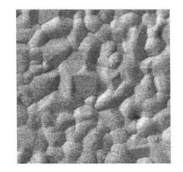
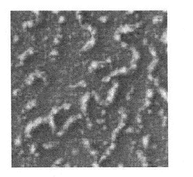
[0045] The MIM capacitor proposed by the present invention and its preparation method will be further described in detail below in conjunction with the accompanying drawings and specific embodiments. Advantages and features of the present invention will be apparent from the following description and claims. It should be noted that all the drawings are in very simplified form and use imprecise ratios, which are only used for the purpose of conveniently and clearly assisting in describing the embodiments of the present invention.

[0046] The core idea of ​​the present invention is to provide a kind of MIM capacitor, the grain size of the metal of the first conductive layer and the second conductive layer of the capacitor is 1.2um~2.5um, thereby reducing the MIM capacitor produced in the etching process The problem of metal residue; at the same time, a method for preparing MIM capacitors is provided. In the MIM capacitors prepared by this method, the grain size of the metal in t...


PUM

PropertyMeasurementUnit
Grainaaaaaaaaaa
Thicknessaaaaaaaaaa
Thicknessaaaaaaaaaa

Abstract

The invention discloses a metal-insulator-metal (MIM) capacitor. The grain size of metal of a first conductive layer and a second conductive layer of the capacitor is 1.2 to 2.5mu m, so that the problem of metal residues generated in the process of etching the MIM capacitor is solved. Meanwhile, the invention discloses a preparation method for the MIM capacitor. The idle time of a sputtering machine table is detected before each lot of chips are subjected to metal sputtering by the method, so that the problem of the metal residues generated in the etching process due to too small grains of the sputtered metal caused by low process stability of the sputtering machine table is solved.

Description

technical field [0001] The invention relates to the technical field of semiconductor integrated circuit preparation, in particular to a MIM capacitor and a preparation method thereof. Background technique [0002] Passive Circuit Elements such as capacitors and resistors are widely used in integrated circuit manufacturing technology. These devices usually use standard integrated circuit technology, using doped single crystal silicon, doped polycrystalline silicon, and oxide film or oxynitride film. into, such as polysilicon-dielectric film-polysilicon (PIP, Poly-Insulator-Poly) capacitance. Because these devices are relatively close to the silicon substrate, the parasitic capacitance between the device and the substrate affects the performance of the device, especially in radio frequency (RF) CMOS circuits, as the frequency increases, the performance of the device decreases rapidly. [0003] The development of metal-insulator-metal (MIM, Metal-Insulator-Metal) capacitor tec...

Claims


Application Information

Patent Timeline
IPC IPC(8): H01L29/92H01L21/334
Inventor 牛健李广福杨林宏
Owner SEMICONDUCTOR MANUFACTURING INTERNATIONAL (BEIJING) CORP
Learn More