LED outputting narrow-band notch filtering light and preparation method thereof

A light-emitting diode and wave trap technology, applied in the directions of diffraction gratings, electrical components, circuits, etc., to achieve the effect of convenient peak and narrow-band bandwidth, protection of metal film layer, and convenient adjustment

Active Publication Date: 2014-07-02
苏州东辉光学有限公司
View PDF7 Cites 0 Cited by
  • Summary
  • Abstract
  • Description
  • Claims
  • Application Information

AI Technical Summary

Problems solved by technology

However, so far, the idea of ​​designing the structure of the LED chip itself in order to achieve a highly integrated and efficient active filter device has not been reported.

Method used


Image

  • LED outputting narrow-band notch filtering light and preparation method thereof
  • LED outputting narrow-band notch filtering light and preparation method thereof
  • LED outputting narrow-band notch filtering light and preparation method thereof

Examples


Embodiment 1

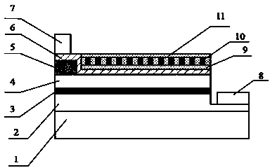
[0037] See attached figure 1 , which is a structural cross-sectional schematic diagram of an active narrow-band notch filter based on a sub-wavelength metal composite grating embedded in a light-emitting diode provided in this embodiment. The structure of the multilayer waveguide active notch filter light-emitting diode chip prepared on the surface of the III-V gallium nitride-based LED is as follows: an LED light-emitting working area is grown on the substrate material 1, including n-type GaN area 2, p type GaN region 4 and InGaN / GaN quantum well 3; on the p-type GaN region there is an insulating dielectric film 5 in sequence, and the insulating medium is SiO 2 Or SiN; p-type layer transparent electrode 6; p-type layer metal electrode 7 and n-type layer metal electrode 8; dielectric transition layer 9 and dielectric protection layer 11, the dielectric layer is the same or different materials, which can be SiO 2 、Al 2 o 3 , MgF 2 , ZnS, ZnO, BK7 glass and other transparent...

Embodiment 2

[0042] In this embodiment, a multi-layer waveguide trap wave emitting light-emitting diode chip with different periods of the composite grating is prepared.

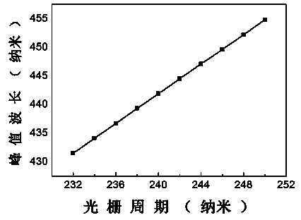
[0043] According to different filter light center wavelengths, adopt the technical scheme of embodiment 1, obtain the dielectric transition layer thickness of the diode chip to be 160nm, the composite grating thickness is 210nm, the duty ratio is 0.5, the dielectric protection layer thickness is 10nm, the period of the composite grating They are 232nm, 234nm, 236nm, 238nm, 240nm, 242nm, 244nm, 246nm, 248nm and 250nm.

[0044] See attached image 3 , which is a graph showing the change of the notch spectral peak of the light-emitting diode chip provided by this embodiment in the light-emitting wavelength range of about 30 nanometers as the period of the composite grating changes. Depend on image 3 It can be seen that the period of the grating changes by 18nm, and the peak position of the notch spectrum moves by 23.3nm ...

Embodiment 3

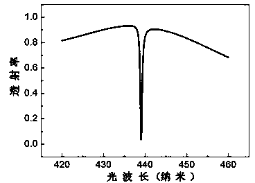
[0046] According to different bandwidths, the technical solution of Embodiment 1 is adopted to obtain the thickness of the dielectric transition layer of the multilayer waveguide type trap light emitting diode chip provided by this embodiment, the thickness of the dielectric transition layer is 160nm, the thickness of the composite grating is 210nm, the period is 240nm, and the thickness of the dielectric protection layer is 10nm. The corresponding composite grating duty ratios are 0.35, 0.45 and 0.55, respectively.

[0047] See attached Figure 4 , which is a graph of the transmittance curves of different filter bandwidths of the notch narrowband spectrum of the light emitting diode chip provided in this embodiment in the 430nm-450nm light emission band under different duty ratio conditions of the composite grating. Depend on Figure 4 It can be seen that the thickness of the dielectric transition layer of the multi-layer waveguide trap light-emitting diode chip provided in ...


PUM


Abstract

The invention discloses an LED outputting narrow-band notch filtering light, and a preparation method thereof. According to the invention, a multi-layer waveguide structural layer is composited on the light-emitting surface of an LED chip and comprises a medium depletion layer, a composite grating layer and a medium protective layer; the composite grating layer is a metal / medium grating film layer which is formed by metal strips and medium strips at intervals; the medium depletion layer is positioned below the composite grating layer and is in direct contact with the light-emitting surface of the LED chip; the medium protective layer is above the composite grating layer and is in direct contact with the ambient environment or transparency electrode; and the thickness of each layer of the multi-layer waveguide structure layer, the grating duty cycle and the period parameter are designed to meet the condition of the resonance of the light waveguide mold transmission. According to the invention, a sub-wavelength metal / medium composite grating structure is directly integrated on the surface of the LED chip, and the LED per se has filtering effect; and compared with a traditional passive filter, the LED is a highly integrated active filtering light-emitting device.

Description

technical field [0001] The invention relates to a light-emitting diode (LED) light source that generates light with a semiconductor band gap structure, in particular to an electromagnetic wave transmission structure, a narrow-band filter light source with an embedded sub-wavelength composite grating structure, and belongs to the field of micro-nano optical devices. Background technique [0002] With the rapid development of nanolithography technology and people's urgent need for miniaturization of optical components and integration of optical systems, the research, design and preparation of micro-nano optical devices have become a hot spot of widespread concern in academia and industry. Micro-nano optical components continue to emerge. The main function of optical filters is to filter specific wavelength light sources within the working band and cut off incident light of other wavelengths. The main structure of the traditional optical filter is to vapor-deposit multiple...

Claims


Application Information

Patent Timeline
Patent Type & Authority Patents(China)
IPC IPC(8): H01L33/00G02B5/18
Inventor 张桂菊曹冰王钦华
Owner 苏州东辉光学有限公司
Why Eureka
Try Eureka