Power supply management circuit, power supply management module and power supply management method thereof
A power management module and power management technology, applied in battery circuit devices, circuit devices, current collectors, etc., to avoid mutual charging
- Summary
- Abstract
- Description
- Claims
- Application Information
AI Technical Summary
Problems solved by technology
Method used
Image

Examples
no. 1 example
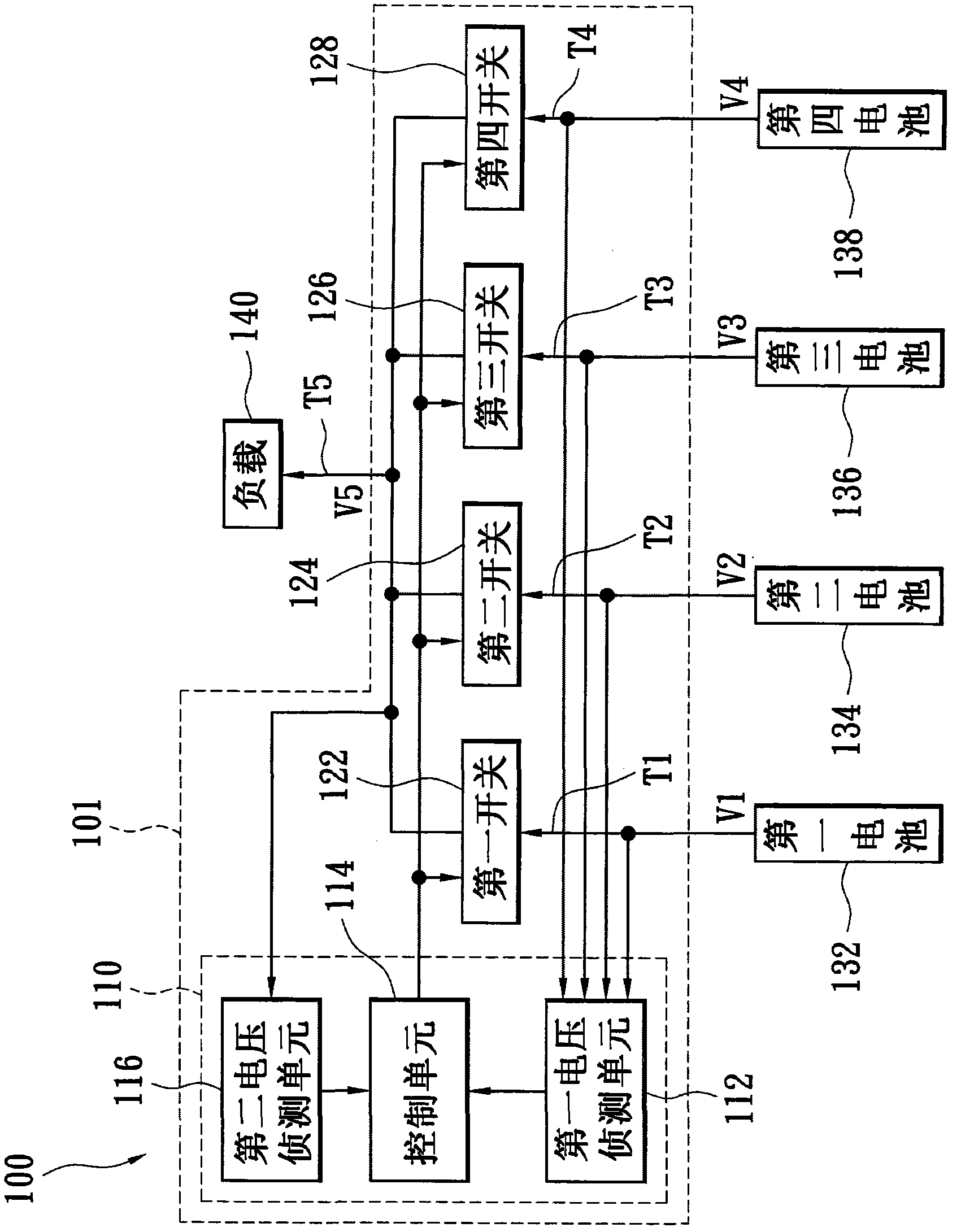
[0034] figure 1 It is a schematic diagram of the power management module according to the first embodiment of the present invention. The power management module 100 includes a power management circuit 101 and a plurality of batteries (a first battery 132 , a second battery 134 , a third battery 136 and a fourth battery 138 ). The power management circuit 101 is coupled between the first to the fourth batteries 132-138 and the load 140, and selectively conducts the first to the fourth batteries according to the voltages of the output terminals T1-T4 of the first to the fourth batteries and the load terminal T5. The four switches 122 - 128 allow the first to fourth batteries 132 - 138 to supply power to the load 140 .
[0035] The power management circuit 101 includes an output control unit 110 and first to fourth switches 122 - 128 , wherein the output control unit 110 further includes a first voltage detection unit 112 , a control unit 114 and a second voltage detection unit ...
no. 2 example
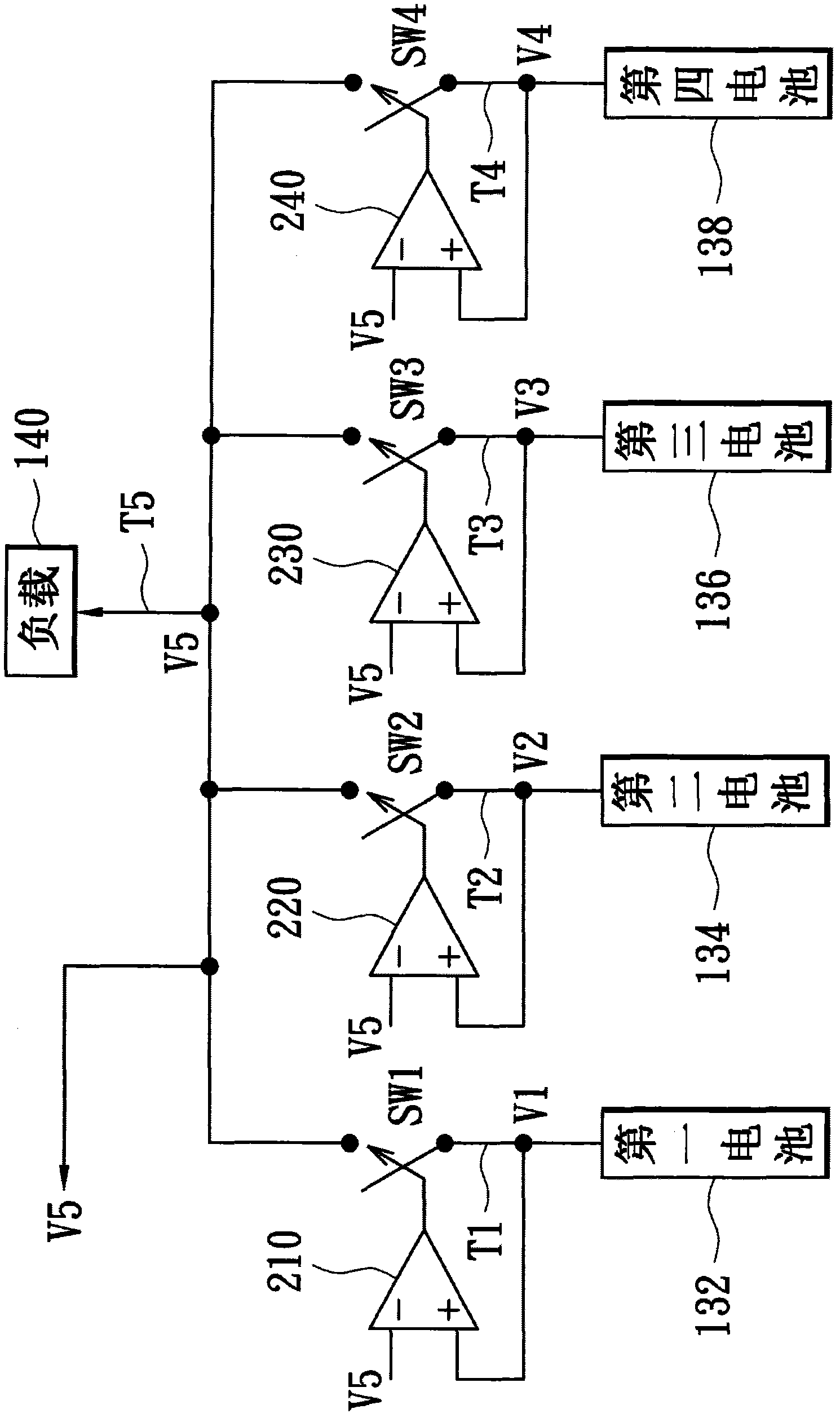
[0043] Please refer to figure 1 and image 3 , image 3 It is a schematic circuit diagram of the power management module according to the second embodiment of the present invention. In the second embodiment of the present invention, the above-mentioned output control unit 110 can be implemented by two resistors R1 - R8 connected in series, and the first to fourth switches 122 - 128 are implemented by PMOS transistors P1 - P4 . Sources of the PMOS transistors P1 - P4 are respectively coupled to the first to fourth battery output terminals T1 - T4 , and drains of the PMOS transistors P1 - P4 are coupled to the load 140 . Resistors R1 and R2 are coupled in series between the load terminal T5 and the first battery output terminal T1, and their shared contact is coupled to the gate of the PMOS transistor P1; resistors R3 and R4 are coupled in series between the load terminal T5 and the second battery output Between terminals T2, its shared contact is coupled to the gate of the P...
no. 3 example
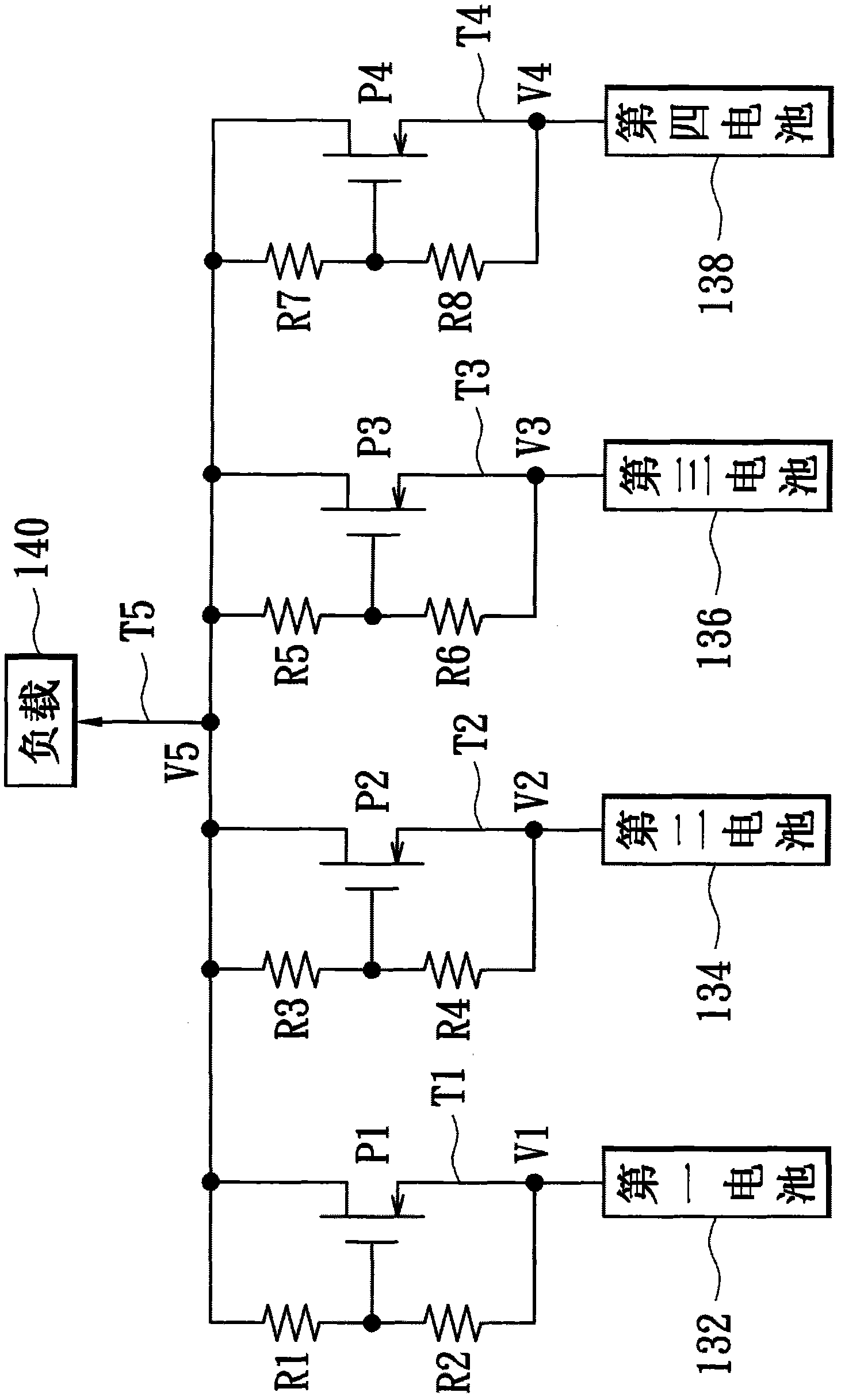
[0046] Please refer to figure 1 and Figure 4 , Figure 4 is a schematic circuit diagram of a power management module according to a third embodiment of the present invention. In the second embodiment of the present invention, the above-mentioned power management circuit 101 can be implemented by using two resistors R1 - R8 connected in series, and the first to fourth switches 122 - 128 are implemented by NMOS transistors N1 - N4 . Figure 4 and image 3 The main difference lies in the NMOS transistors N1-N4, because the NMOS transistors N1-N4 are driven by a positive gate-source voltage. Therefore, the sources of the NMOS transistors N1-N4 are respectively coupled to the load terminal T5, and their drains are respectively coupled to the first to fourth battery output terminals T1-T4, and their gates are respectively coupled to the resistors R1-R8. Shared joints. For example, when the voltage V1 is greater than the voltage V5 and the difference is greater than the thresho...
PUM
 Abstract
Description
Claims
Application Information
 - R&D
- Intellectual Property
- Life Sciences
- Materials
- Tech Scout
- Unparalleled Data Quality
- Higher Quality Content
- 60% Fewer Hallucinations
Browse by: Latest US Patents, China's latest patents, Technical Efficacy Thesaurus, Application Domain, Technology Topic, Popular Technical Reports.
© 2025 PatSnap. All rights reserved.Legal|Privacy policy|Modern Slavery Act Transparency Statement|Sitemap|About US| Contact US: help@patsnap.com