Method for manufacturing X-ray sensor
A sensor and X-ray technology, applied in the field of X-ray sensor production, can solve the problems of high product cost, low yield and low equipment capacity.
- Summary
- Abstract
- Description
- Claims
- Application Information
AI Technical Summary
Problems solved by technology
Method used
Image

Examples
Embodiment Construction
[0036] Aiming at the problems of high product cost, low yield rate and low equipment productivity caused by too many mask exposure times in the process of manufacturing X-ray sensors in the prior art, an embodiment of the present invention provides an X-ray sensor and its production method.
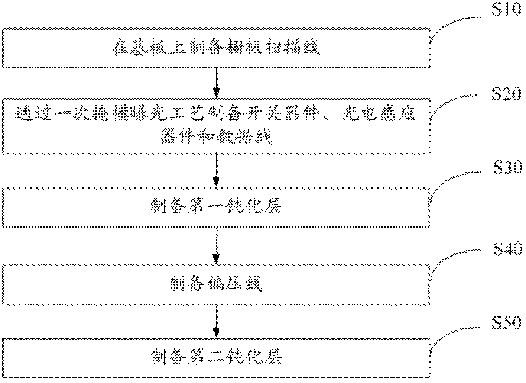
[0037] The manufacturing method of the X-ray sensor provided by the embodiment of the present invention, its process is as follows image 3 shown, including the following steps:
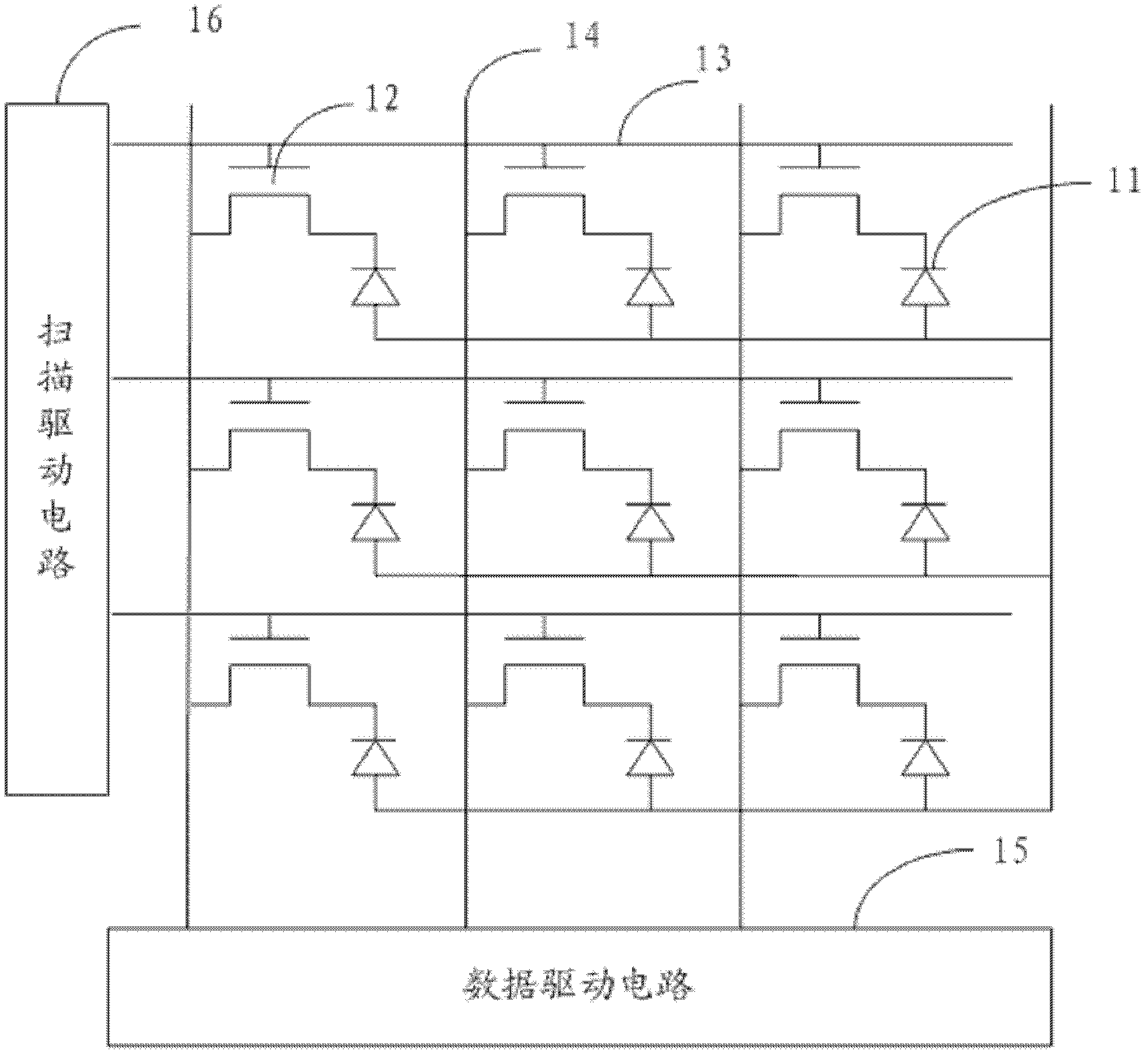
[0038] Step S10: preparing at least two gate scanning lines on the substrate; each gate scanning line serves as a gate of a switching device included in a row of pixel units in the X-ray sensor.
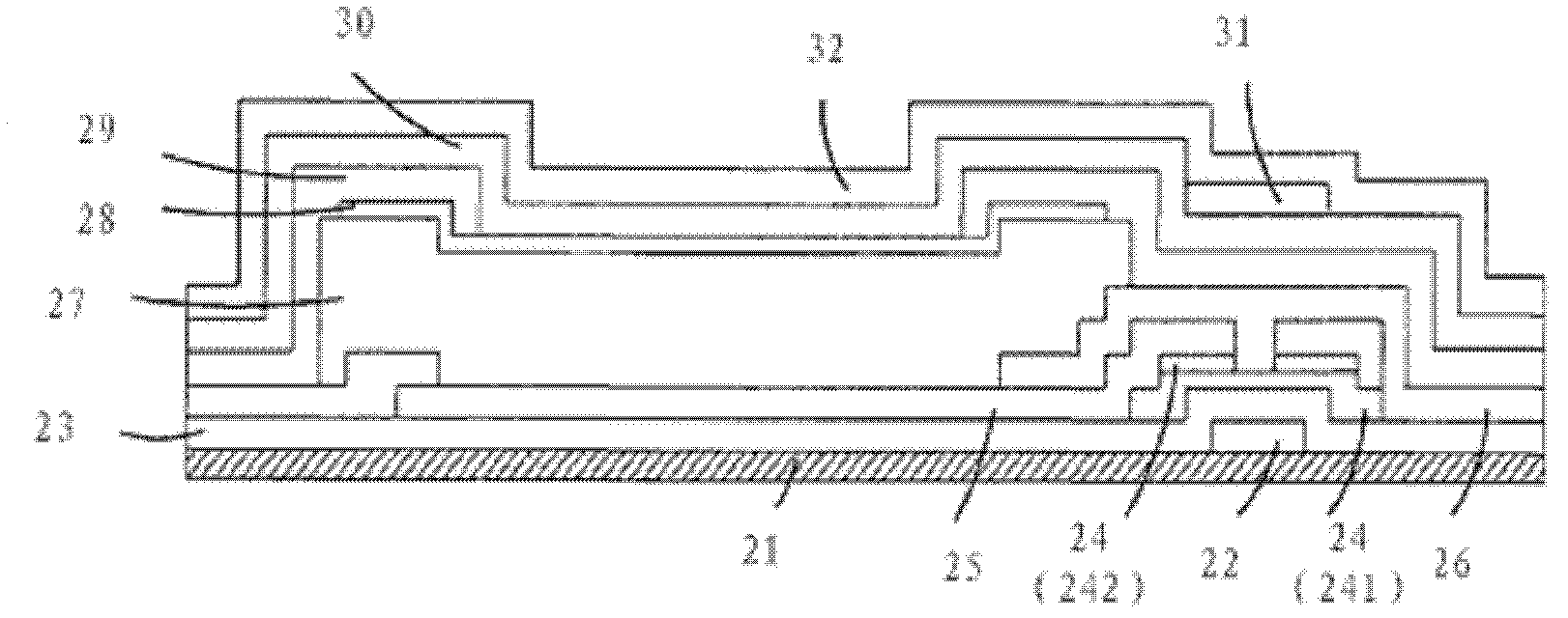
[0039] Step S20: sequentially depositing a gate insulating layer, an active layer film, an ohmic contact layer film, a first conductive layer film, and a photoelectric conversion layer film on the substrate and the gate scanning line; for the active layer film, the ohmic contact layer film, the second A conductive la...
PUM
 Abstract
Description
Claims
Application Information
 - R&D Engineer
- R&D Manager
- IP Professional
- Industry Leading Data Capabilities
- Powerful AI technology
- Patent DNA Extraction
Browse by: Latest US Patents, China's latest patents, Technical Efficacy Thesaurus, Application Domain, Technology Topic.
© 2024 PatSnap. All rights reserved.Legal|Privacy policy|Modern Slavery Act Transparency Statement|Sitemap