Method for reducing grid-induction drain leakage of semiconductor device

A semiconductor and drain leakage technology, applied in semiconductor devices, semiconductor/solid-state device manufacturing, electrical components, etc., can solve problems such as complex processes, reduce the width of the sidewall, reduce the drain leakage current, and increase the sidewall effect of width

Inactive Publication Date: 2012-08-15
SHANGHAI HUALI MICROELECTRONICS CORP
View PDF5 Cites 0 Cited by
  • Summary
  • Abstract
  • Description
  • Claims
  • Application Information

AI Technical Summary

Problems solved by technology

This method is more complex

Method used


Image

  • Method for reducing grid-induction drain leakage of semiconductor device
  • Method for reducing grid-induction drain leakage of semiconductor device
  • Method for reducing grid-induction drain leakage of semiconductor device

Examples


Embodiment Construction

[0024] The present invention will be further described below in combination with principle diagrams and specific operation examples.

[0025] see figure 2 As shown, the method for reducing gate-induced drain leakage of semiconductor devices in the present invention specifically includes the following steps:

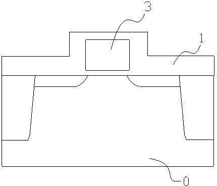
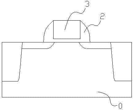
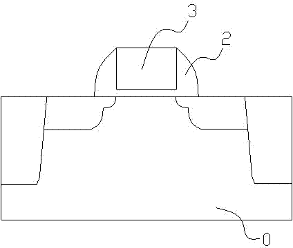
[0026] Such as Figure 3A As shown, a layer of sidewall film 1 is grown on a substrate 0 that has completed shallow trench isolation (STI) 4 on both sides. The sidewall film 1 can be a silicon oxide or silicon nitride film. There are low doped source and drain regions (LDD) 8 at the junction with the gate, and at the junction between the drain and the gate respectively. The sidewall film 1 is dry-etched, specifically, the sidewall film 1 is dry-etched using anisotropic plasma, and the introduced etching plasma 5 is incident on the source electrode 7. point and form a certain angle α with the vertical direction to form a spacer 2 on the gate 3 of the semiconductor devi...


PUM


Abstract

The invention discloses a method for reducing grid-induction drain leakage of a semiconductor device. The method includes steps: growing a side-wall film on a substrate with completed two-side shallow trench isolation; etching the side-wall film, guiding etching plasma to advance towards an incident point of a source electrode, forming a certain angle between the etching plasma and the vertical direction, forming a side wall on a grid electrode of the semiconductor device, reducing the width of the etched side-wall source electrode, and widening a drain electrode; and realizing heavy doping for the source electrode and the drain electrode and an annealing process. By the aid of the method, the intensity of a longitudinal electric field on a leaked end is reduced under the condition of keeping the effective lengths of trenches unchanged, and accordingly grid-caused leakage current of the drain electrode of the semiconductor device is reduced.

Description

technical field [0001] The invention relates to the technical field of semiconductor preparation, in particular to a method for reducing gate-induced drain leakage of semiconductor devices. Background technique [0002] Gate-Induced Drain Leakage (GIDL, Gate-Induced Drain Leakage) means that when the device is off-state (ie Vg=0), if the drain is connected to Vdd (ie Vd=Vdd), Due to the overlap between the gate and the drain, there will be a strong electric field in the overlapping region between the gate and the drain, and the carriers will undergo band-to-band tunneling under the action of the strong electric field. Tunneling), causing leakage current from drain to gate. [0003] The gate-induced-drain leakage current has become one of the main reasons affecting the reliability and power consumption of small-sized MOS devices, and it also has an important impact on the erasing and writing operations of memory devices such as EEPROM. When the process enters the ultra-deep...

Claims


Application Information

Patent Timeline
IPC IPC(8): H01L21/336
CPCH01L29/66659H01L29/7835
Inventor 俞柳江
Owner SHANGHAI HUALI MICROELECTRONICS CORP
Why Eureka
Try Eureka