Method for reducing semiconductor device hot carrier injection damage

A technology of hot carrier and injection damage, applied in semiconductor devices, semiconductor/solid-state device manufacturing, electrical components, etc., can solve the problem of easy failure of drain terminals

Active Publication Date: 2012-05-02
SHANGHAI HUALI MICROELECTRONICS CORP
View PDF5 Cites 1 Cited by
  • Summary
  • Abstract
  • Description
  • Claims
  • Application Information

AI Technical Summary

Problems solved by technology

[0006] For the semiconductor device manufactured by the above method, the sidewall thickness of the drain end and the source end around the gate is the same, and the distance between t

Method used


Image

  • Method for reducing semiconductor device hot carrier injection damage
  • Method for reducing semiconductor device hot carrier injection damage
  • Method for reducing semiconductor device hot carrier injection damage

Examples


Embodiment Construction

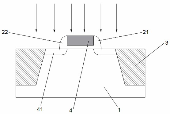
[0030] The present invention provides a method for reducing hot carrier injection damage of a semiconductor device, and a semiconductor device fabricated by using the method. In the sidewall etching process, the plasma introduction direction for etching is not perpendicular to the substrate surface, and the plasma introduction direction is inclined from the source end of the gate to the drain end; the plasma introduction direction is not perpendicular to the substrate surface The included angle is greater than 45 degrees and less than 90 degrees.

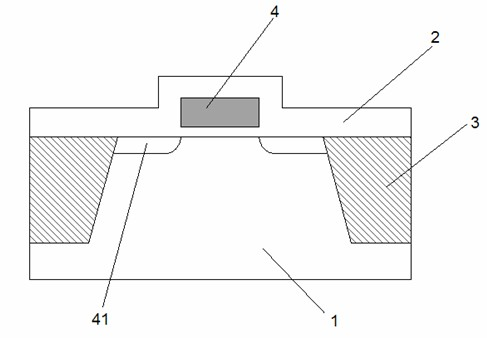
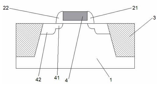
[0031] 1 and 2, the method for reducing the hot carrier injection damage of a semiconductor device of the present invention and the semiconductor device fabricated by using the method of the present invention are described in detail by taking the manufacture of a 55nm CMOS device as an example, so as to make a better understanding of the present invention, but the following examples do not limit the scope of the present invention. ...


PUM

PropertyMeasurementUnit
Angleaaaaaaaaaa

Abstract

The invention provides a method for reducing the semiconductor device hot carrier injection damage. In a spacer etching process, an inclined angle introduction plasma etching method is adopted, so the spacer width of the drain end after the etching is increased, the spacer width of the source end is decreased, after the subsequent source and drain high doping injection and annealing process, the distance from doped ions of the drain end to a channel is enlarged, the distance from doped ions of the source end to the channel and a substrate is reduced, under the condition of keeping the effective channel length unchanged, and the longitudinal electric field intensity of the drain end is reduced, so the semiconductor device hot carrier injection damage is reduced.

Description

technical field [0001] The present invention relates to a manufacturing method of a semiconductor device, in particular to a method for reducing hot carrier injection damage of a semiconductor device, and a semiconductor device manufactured using the method. Background technique [0002] With the improvement of the integration of miniaturized systems, the size of metal oxide semiconductor (MOS) devices has been drastically reduced. The high integration of the device and the ultra-thin gate oxide layer enable the device to provide better performance. The shortening of the gate oxide layer and the thinning of the gate oxide layer will bring a series of reliability problems to the fabricated MOS device. [0003] Hot carrier effect is an important failure mechanism of MOS devices. As the size of MOS devices shrinks, the hot carrier injection effect of devices becomes more and more serious. Taking a PMOS device as an example, the holes in the channel are accelerated by the high ...

Claims


Application Information

Patent Timeline
IPC IPC(8): H01L21/336H01L29/78
Inventor 俞柳江
Owner SHANGHAI HUALI MICROELECTRONICS CORP
Why Eureka
Try Eureka