Supercharge Your Innovation With Domain-Expert AI Agents!

Semiconductor device with overvoltage protection and bidirectional polarity device based on it

An overvoltage protection, semiconductor technology, applied in the direction of semiconductor devices, electrical components, circuits, etc., can solve the problems of device damage, uneven current density of PN junction, etc., to achieve the effect of high reliability and high overcurrent bearing capacity

Active Publication Date: 2016-02-03
汇立装备制造有限公司
View PDF6 Cites 0 Cited by
  • Summary
  • Abstract
  • Description
  • Claims
  • Application Information

AI Technical Summary

Problems solved by technology

[0006] It can be seen that during the conduction process of this kind of device, the PN junction current density between each N+ type region 3 and P type region 2 is not uniform, and the conduction first occurs in the N+ type region closest to the P+ type region 2 5 At the boundary of -3, the PN junction current density between the N+-type region-3 and the P-type region-2 will easily and quickly reach the critical value that the semiconductor material can withstand, resulting in device damage

Method used


Image

  • Semiconductor device with overvoltage protection and bidirectional polarity device based on it
  • Semiconductor device with overvoltage protection and bidirectional polarity device based on it
  • Semiconductor device with overvoltage protection and bidirectional polarity device based on it

Examples


Embodiment 1

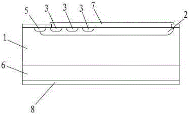
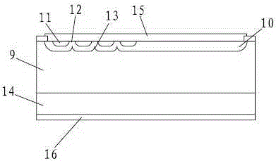
[0034] Example 1: Such as figure 2 As shown, a semiconductor device with overvoltage protection includes a substrate 9 having a first conductivity type,

[0035] A first region 10 of the second conductivity type provided on the upper part of the substrate 9,

[0036] A plurality of second regions 11 of the first conductivity type arranged on the upper part of the first region 10,

[0037] A third region 14 of the second conductivity type provided on the lower surface of the substrate 9,

[0038] The first metal contact 15 connected to the first area 10 and the second area 11,

[0039] A second metal contact 16 connected to the third area 14;

[0040] The substrate 9 has a plurality of undulating regions 13 at the junction with the lower surface of the first region 10; the first region 10 forms a first opening region 12 between adjacent second regions 11, and each undulating region 13 All correspond to the middle of the first opening area 12.

[0041] The first conductivity type is N typ...

Embodiment 2

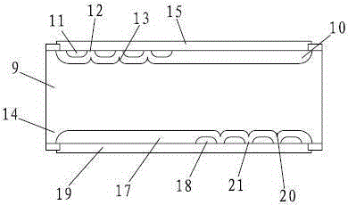
[0045] Embodiment 2: A bidirectional polar semiconductor device with overvoltage protection, which includes a substrate 9 of the first conductivity type,

[0046] A first region 10 of the second conductivity type disposed on the upper part of the substrate 9,

[0047] A fourth region 17 of the second conductivity type located under the substrate 9,

[0048] A plurality of second regions 11 which are provided on the upper part of the first region 10 and are all of the first conductivity type,

[0049] A plurality of fifth regions 18 that are provided under the fourth region 17 and are all of the first conductivity type,

[0050] The first metal contact 15 connected to the first area 10 and the second area 11,

[0051] The third metal contact 19 connected to the fourth area 17 and the fifth area 18;

[0052] The substrate 9 has a plurality of undulating regions 13 at the interface with the lower surface of the first region 10; the substrate 9 has a plurality of recessed regions 20 at the in...


PUM


Abstract

The invention relates to a semiconductor apparatus, and in particular relates to a semiconductor apparatus with overvoltage protection and a bidirectional polar device based on the apparatus. The invention is realized by the following scheme: the semiconductor apparatus with overvoltage protection comprises a substrate, a first area arranged on the substrate, a plurality of second areas arranged at the upper part of the first area, a third area arranged on the lower surface of the substrate, a first metal contact connected on the first area and the second area, and a second metal contact connected on the third area, a plurality of fluctuation areas are arranged at the junction of the lower surfaces of the substrate and the first area, and each fluctuation area corresponds to the middle of the second area. Compared with the background art, when the semiconductor apparatus is conducted, the current density of a PN knot close to the breakdown cathode and the cathode base region has difficulty in achieving the critical value endured by a semiconductor material, so that excess current endurance is improved, and the apparatus works more reliably.

Description

Technical field [0001] The invention relates to a semiconductor device, in particular to a semiconductor device with overvoltage protection and a bidirectional polar device based on the device. Background technique [0002] Known semiconductor devices with overvoltage protection have a lower breakdown voltage region located close to the junction between the adjacent cathode base region and the anode base region, as described in the US Patent No. 4,282,555 of P. Svedberg A low-voltage protection method for semiconductor devices is disclosed. [0003] This region has the same conductivity type as the cathode base region, but has a higher doping concentration than the cathode base region, and due to the high doping concentration of this region, the electric field strength of the PN junction between this region and the adjacent anode base region is higher than The electric field strength of the PN junction at the junction of the anode base region and the cathode base region, therefore...

Claims


Application Information

Patent Timeline
Patent Type & Authority Patents(China)
IPC IPC(8): H01L29/45H01L29/06
Inventor 谢可勋西里奥·艾·珀里亚科夫
Owner 汇立装备制造有限公司
Features
  • R&D
  • Intellectual Property
  • Life Sciences
  • Materials
  • Tech Scout
  • Unparalleled Data Quality
  • Higher Quality Content
  • 60% Fewer Hallucinations
Learn More