Image sensor detection device and method

An image sensor, a technology for detecting images, applied in image communication, parts of color TVs, parts of TV systems, etc., can solve problems such as the influence of interpolation accuracy, and achieve the effect of improving image quality

Active Publication Date: 2012-09-19
SHANGHAI MICRO ELECTRONICS EQUIP (GRP) CO LTD
View PDF6 Cites 14 Cited by
  • Summary
  • Abstract
  • Description
  • Claims
  • Application Information

AI Technical Summary

Problems solved by technology

In the patent CN200810112796.4, multiple pixels around the bad pixel are used to interpolate the bad pixel, avoiding the influence of bad pixels directly adjacent to each other, but when there is a dense distribution of bad pixels in a certain area, Interpolation accuracy will still suffer

Method used


Image

  • Image sensor detection device and method
  • Image sensor detection device and method
  • Image sensor detection device and method

Examples


Embodiment Construction

[0017] Specific embodiments of the present invention will be described in detail below with reference to the accompanying drawings.

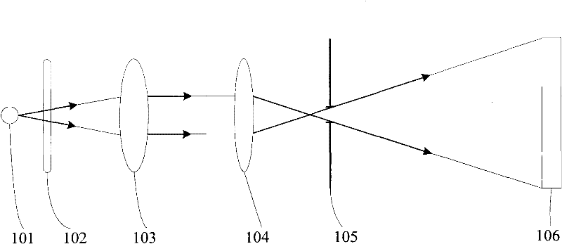
[0018] like figure 1 shown in, figure 1 The invention relates to a device for detecting an image sensor, which is simple in structure, low in cost and very easy to implement. The detection device sequentially includes a light source 101 , an optical attenuator 102 , a first lens group 103 , a second lens group 104 , a diaphragm 105 and an image sensor 106 according to the propagation direction of the optical path. The light emitted from the light source 1 passes through the optical attenuator 102 to generate a suitable detection illumination intensity. The optical attenuator 102 is a device used for attenuating optical power, and in this embodiment, an attenuating sheet with a simple structure is preferably used for schematic illustration. The light beam coming out of the attenuation plate 102 is converted into parallel light after passing th...


PUM


Abstract

The invention discloses an image sensor detection device sequentially comprising a light source, an optical attenuator, a first lens group, a second lens group, a diaphragm and an image sensor along an optical propagation direction. Exposure images of the image sensor under different light intensities are obtained by adjusting the transmissivity of the optical attenuator. The invention also discloses an image sensor detection method comprising the following steps of: obtaining the exposure images of the sensor under the different light intensities under the different light intensities; calibrating defective pixels of the sensor according to the obtained exposure images; calibrating bad cluster areas of the sensor according to the definition of bad clusters, and sequencing the bad cluster areas to find the area with a good measuring effect.

Description

technical field [0001] The present invention relates to a detection device and a detection method for image equipment, in particular to a detection device and detection method for an image sensor. Background technique [0002] Image sensor is an important part of digital camera. According to different components, it can be divided into two categories: CCD (ChargeCoupled Device, charge coupled device) and CMOS (Complementary Metal-Oxide Semiconductor, metal oxide semiconductor device). [0003] Due to the limitation of the manufacturing process, there are inevitably some defects in the currently manufactured image sensor, such as the existence of bad pixels (hereinafter referred to as bad pixels). A dead pixel generally means that the dark current of the pixel is too large or its gain is significantly different from that of other pixels. The existence of a dead pixel is one of the reasons for the degradation of image quality. In the prior art, the above-mentioned defects ar...

Claims


Application Information

Patent Timeline
Patent Type & Authority Applications(China)
IPC IPC(8): H04N17/00H04N5/357
Inventor 葛亮王帆
Owner SHANGHAI MICRO ELECTRONICS EQUIP (GRP) CO LTD
Why Eureka
Try Eureka