
Semiconductor device and method for manufacturing same

A manufacturing method, semiconductor technology, applied in semiconductor/solid-state device manufacturing, semiconductor devices, electrical components, etc., can solve problems such as increased parasitic capacitance

Inactive Publication Date: 2012-09-26
KK TOSHIBA
View PDF3 Cites 16 Cited by
  • Summary
  • Abstract
  • Description
  • Claims
  • Application Information

AI Technical Summary

Problems solved by technology

However, placing the gate electrode and the source electrode close to each other inside the trench increases the parasitic capacitance between the gate and the source.

Method used


Image

  • Semiconductor device and method for manufacturing same
  • Semiconductor device and method for manufacturing same
  • Semiconductor device and method for manufacturing same

Examples


no. 1 approach

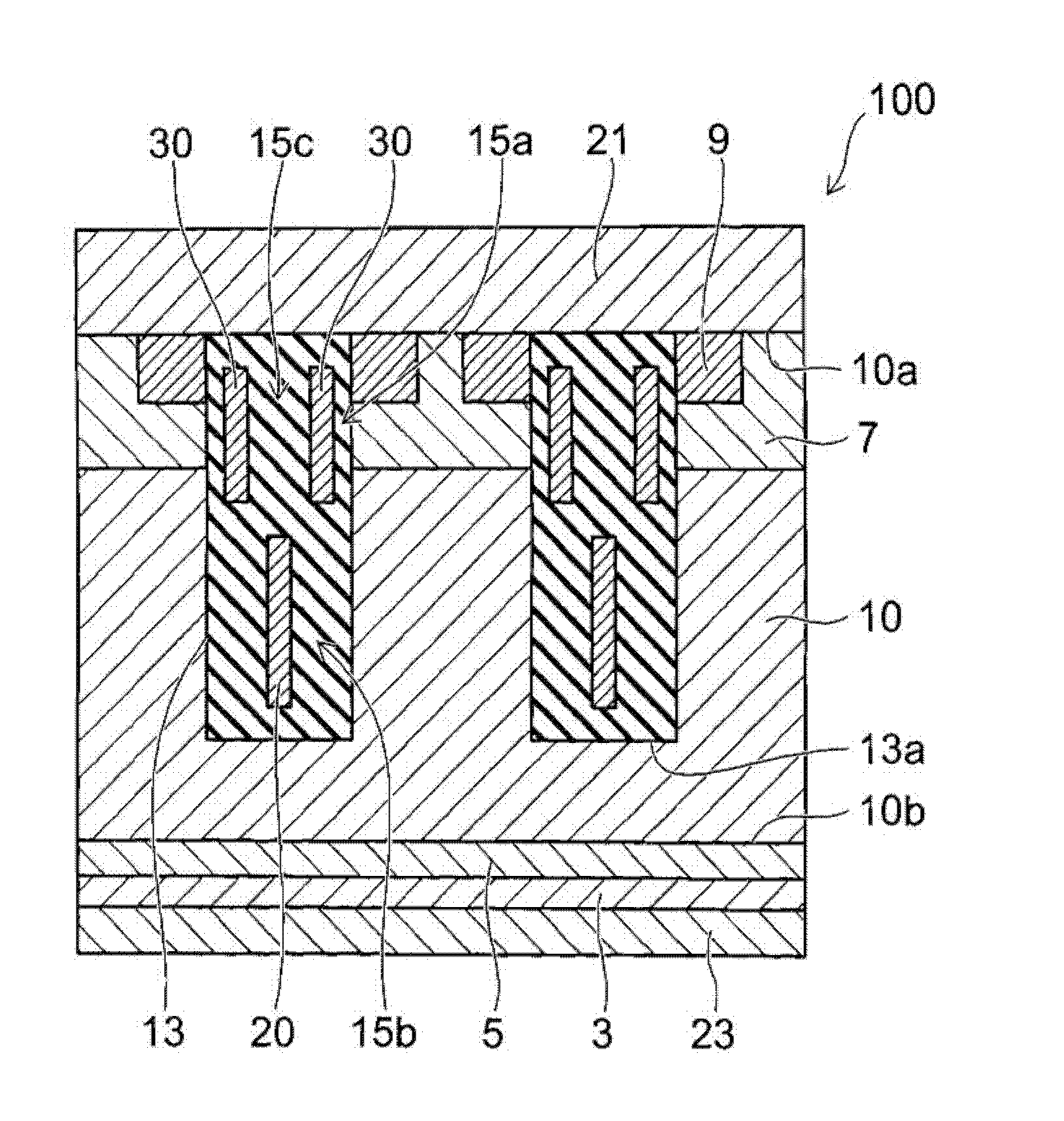
[0020] figure 1 It is a schematic diagram showing the cross-sectional structure of the semiconductor device 100 according to this embodiment. The semiconductor device 100 illustrated here is a power MOSFET having a trench gate structure.

[0021] The semiconductor device 100 has, for example: an n-type drain layer 5 provided on an n-type silicon substrate 3; and a drift layer 10 which is an n-type semiconductor layer. Furthermore, a p-type base region 7 as a first semiconductor region is provided on the surface of the n-type drift layer on the first main surface 10 a side. Furthermore, an n-type source region 9 as a second semiconductor region is provided on the surface of the p-type base region 7 .

[0022] A source electrode 21 as a first main electrode is provided on the first main surface 10 a side of the n-type drift layer 10 . Source electrode 21 is electrically connected to p-type base region 7 and n-type source region 9 .

[0023] On the other hand, a drain electro...

no. 2 approach

[0048] Figure 8 It is a schematic diagram showing the cross-sectional structure of the semiconductor device 300 according to the second embodiment. The semiconductor device 300 is a Schottky barrier diode (SBD) having a trench gate structure, and the Schottky barrier diode (SBD) includes a gate electrode 61 and a field electrode 62 as a second control electrode.

[0049] Such as Figure 8 As shown, the semiconductor device 300 has: an n-type drift layer 10; an anode electrode 41 is a first main electrode arranged on the first main surface 10a side of the n-type drift layer 10; a cathode electrode 43 is arranged on a second main surface 10b side of the second main electrode. A Schottky junction is formed between the anode electrode 41 and the n-type drift layer 10 .

[0050] Further, trench 13 is formed in the direction from the first main surface 10 a side of n-type drift layer 10 toward the second main surface 10 b. Two gate electrodes 61 and a field electrode 62 are pro...

no. 3 approach

[0053] Figure 9 It is a schematic diagram showing a cross-sectional structure of a semiconductor device 400 according to the third embodiment. The semiconductor device 400 is an IGBT (Insulated Gate Bipolar Transistor: Insulated Gate Bipolar Transistor) having a trench gate structure, and has a p-type collector layer 45 and a collector electrode 53 on the second main surface 40b side of the n-type base layer 40. this, with figure 1 The illustrated semiconductor device 100 is different.

[0054] In the semiconductor device 400, a trench gate structure including a field electrode 20, a p-type base region 47 and an n-type emitter region 49, and an emitter electrode 51. Thereafter, the n-type silicon substrate 3 is removed on the side of the second main surface 40b, and the p-type current collecting layer 45 is provided by, for example, ion-implanting p-type impurities. Then, a collector electrode 53 connected to the p-type collector layer is provided.

[0055] Such as Fig...


PUM


Abstract

According to an embodiment, a semiconductor device includes a first semiconductor layer of a first conductive type, a first main electrode provided on a first major surface side of the first semiconductor layer, and a second main electrode provided on a second major surface side of the first semiconductor layer. A pair of first control electrodes is provided within a trench provided from the first major surface side to the second major surface in the first semiconductor layer; and the first control electrodes are provided separately from each other in a direction parallel to the first major surface. Each of the first control electrodes faces an inner face of the trench via a first insulating film. A second control electrode is provided between the first control electrodes and a bottom face of the trench, and faces the inner face of the trench via a second insulating film.

Description

[0001] Cross References to Related Applications [0002] This application is based on and claims priority from prior Japanese Application No. 2011-67631 filed on March 25, 2011, the entire contents of which are incorporated herein by reference. technical field [0003] Embodiments of the present invention relate to a semiconductor device and a method of manufacturing the same. Background technique [0004] Semiconductor devices for power control are widely used as key devices in power electronics. Moreover, it has a structure suitable for various purposes. For example, in applications requiring high-speed switching, high withstand voltage and low on-resistance are desired, and reduction of input capacitance, that is, gate-source capacitance is required. [0005] On the other hand, in order to lower the on-resistance of power semiconductor devices, trench gate structures are widely used. Furthermore, in the trench gate structure, by providing the gate electrode and the sou...

Claims


Application Information

Patent Timeline
Patent Type & Authority Applications(China)
IPC IPC(8): H01L29/78H01L29/739H01L21/336H01L21/331
CPCH01L29/8725H01L29/66734H01L29/42376H01L29/407H01L29/1608H01L29/7813H01L29/41
Inventor 浅原英敏
Owner KK TOSHIBA
Learn More