
Power semiconductor device and method for fabricating same

A technology of power semiconductors and semiconductors, applied in the fields of semiconductor devices, semiconductor/solid-state device manufacturing, electrical components, etc., can solve the problems of increasing switching loss, low device switching speed, etc., to reduce switching loss and gate-source capacitance. , the effect of increasing the switching speed

Pending Publication Date: 2019-05-31
安建科技(深圳)有限公司
View PDF12 Cites 2 Cited by
  • Summary
  • Abstract
  • Description
  • Claims
  • Application Information

AI Technical Summary

Problems solved by technology

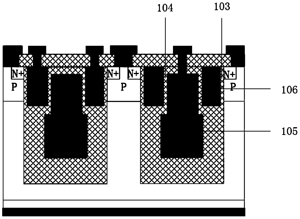
Therefore, the inter-electrode isolation oxide layer (104) formed in the existing shielded gate trench field effect transistor manufacturing process is usually relatively thin, resulting in low switching speed of the device and increased switching loss

Method used


Image

  • Power semiconductor device and method for fabricating same
  • Power semiconductor device and method for fabricating same
  • Power semiconductor device and method for fabricating same

Examples


Embodiment Construction

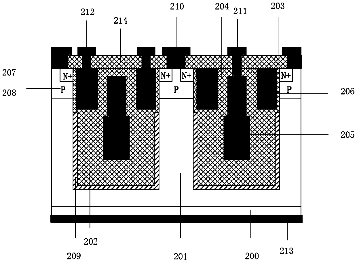
[0043] The present invention will be described in detail below in conjunction with the accompanying drawings and embodiments. It should be pointed out that, in the following description of the shielded gate trench field effect transistor device and its manufacturing method of the present invention, the semiconductor substrate of the shielded gate trench field effect transistor device is considered to be made of silicon (Si) material. However, the substrate can also be made of any other material suitable for manufacturing shielded gate trench field effect transistors, such as gallium nitride (GaN), silicon carbide (SiC) and the like. In the following description, the conductivity type of the semiconductor region is classified into P type (first conductivity type) and N type (second conductivity type). A P-type conductive semiconductor region can be formed by doping one or several kinds of impurities into the original semiconductor region, and these impurities can be but not lim...


PUM


Abstract

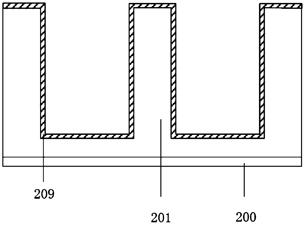
A power semiconductor device and a method for fabricating the same are provided. In order to further increase the switching speed of a shielded gate trench field effect transistor and reduce the switching loss, the invention provides a shield gate trench field effect transistor device structure with a simple fabrication process and a method for fabricating the same. A gate oxide layer and an inter-electrode isolation dielectric layer are respectively formed in different steps, so that the formed inter-electrode isolation dielectric layer is relatively thick, thereby achieving effects of reducing the gate-source capacitance of the device, increasing the switching speed of the device, and reducing the switching loss.

Description

technical field [0001] The invention relates to a structure of a power semiconductor device and a manufacturing method thereof, in particular to a junction of a shielded gate trench type field effect transistor device and a manufacturing method thereof. Background technique [0002] The related technical background of the existing shielded gate trench field effect transistor will be described below. It should be pointed out that the corresponding positional words described in this document such as "upper", "lower", "left", "right", "front", "back", "vertical", "horizontal" are corresponding to the reference The relative position of the icon. The fixed direction is not limited in specific implementation. [0003] Shielded gate trench field effect transistor, as a power device, has the characteristics of low on-resistance and fast switching speed. figure 1 Shown is a schematic diagram of the cross-sectional structure of an N-type shielded gate trench field effect transistor...

Claims


Application Information

Patent Timeline
Patent Type & Authority Applications(China)
IPC IPC(8): H01L29/06H01L29/10H01L29/423H01L21/336H01L29/78
CPCH01L29/407H01L29/7813
Inventor 单建安伍震威梁嘉进袁嵩
Owner 安建科技(深圳)有限公司
Learn More