Semiconductor device and method for manufacturing semiconductor device

a semiconductor and semiconductor technology, applied in semiconductor devices, diodes, transistors, etc., can solve the problem of taking some time for carriers in the p-region pb>2/b> to be discharged, and achieve the effect of enhancing the speed of switching from the on-state to the effective off-sta

Inactive Publication Date: 2007-01-18
SONY CORP
View PDF11 Cites 54 Cited by
  • Summary
  • Abstract
  • Description
  • Claims
  • Application Information

AI Technical Summary

Benefits of technology

[0016] The driving method for the semiconductor device with the above-described structure is the same as that for a thyristor-based semiconductor device in the related art. Specifically, when the semiconductor device is turned on, a forward bias is applied between the electrodes of the first- and second-conductivity-type regions at the both ends. Thus, holes and electrons are recombined at the junction between the first- and second-conductivity-type regions in an intermediate area, which leads to current flow. When the semiconductor device in the on-state is switched to the off-state, a reverse bias is applied to the electrodes of the first- and second-conductivity-type regions at the both ends, and the gate electrode is provided with an intermediate potential between the potentials applied to the both end electrodes. Thus, an electric field is applied to the region coupled to the gate electrode, so that minority...

Problems solved by technology

However, even with this gate electrode based on a MOS structure, similar...

Method used


Image

  • Semiconductor device and method for manufacturing semiconductor device
  • Semiconductor device and method for manufacturing semiconductor device
  • Semiconductor device and method for manufacturing semiconductor device

Examples


first embodiment

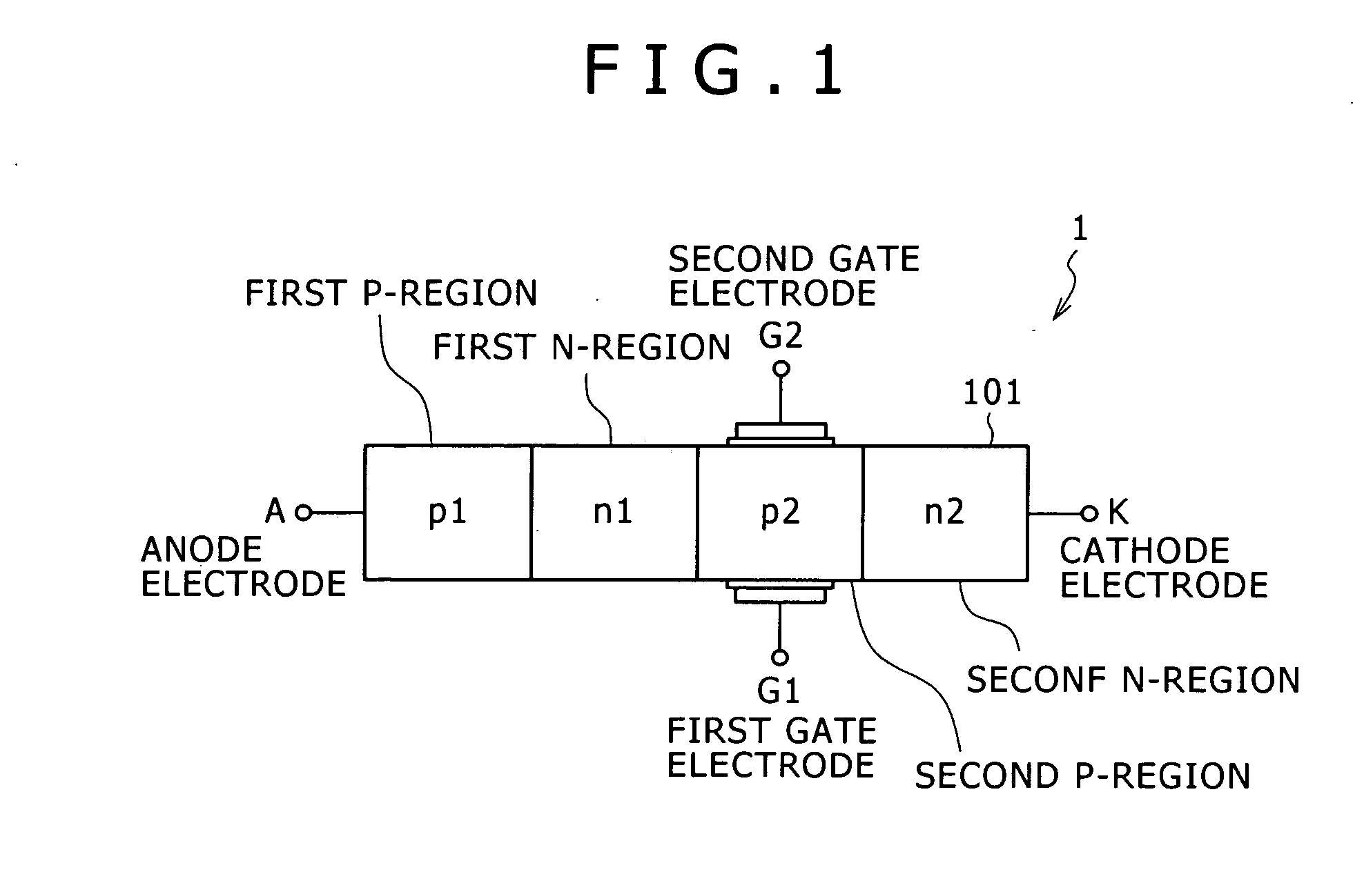
[0035]FIG. 1 is a diagram schematically illustrating the structure of a semiconductor device according to the invention. A semiconductor device 1 shown in FIG. 1 is different from the semiconductor device of the related art described with FIG. 15A, in that gate electrodes G1 and G2 that can be controlled independently of each other are provided over opposed two faces of a p-region p2 formed in an intermediate area of the semiconductor device 1.

[0036] Specifically, the semiconductor device 1 includes a semiconductor layer 101 in which a first p-region p1 (hereinafter, referred to simply as a p-region p1), a first n-region n1 (hereinafter, referred to simply as an n-region n1), a second p-region p2 (hereinafter, referred to simply as a p-region p2), and a second n-region n2 (hereinafter, referred to simply as an n-region n2) are adjacent to each other in that order. Furthermore, an anode electrode A is connected to the p-region p1 at one outermost end, while a cathode electrode K is c...

second embodiment

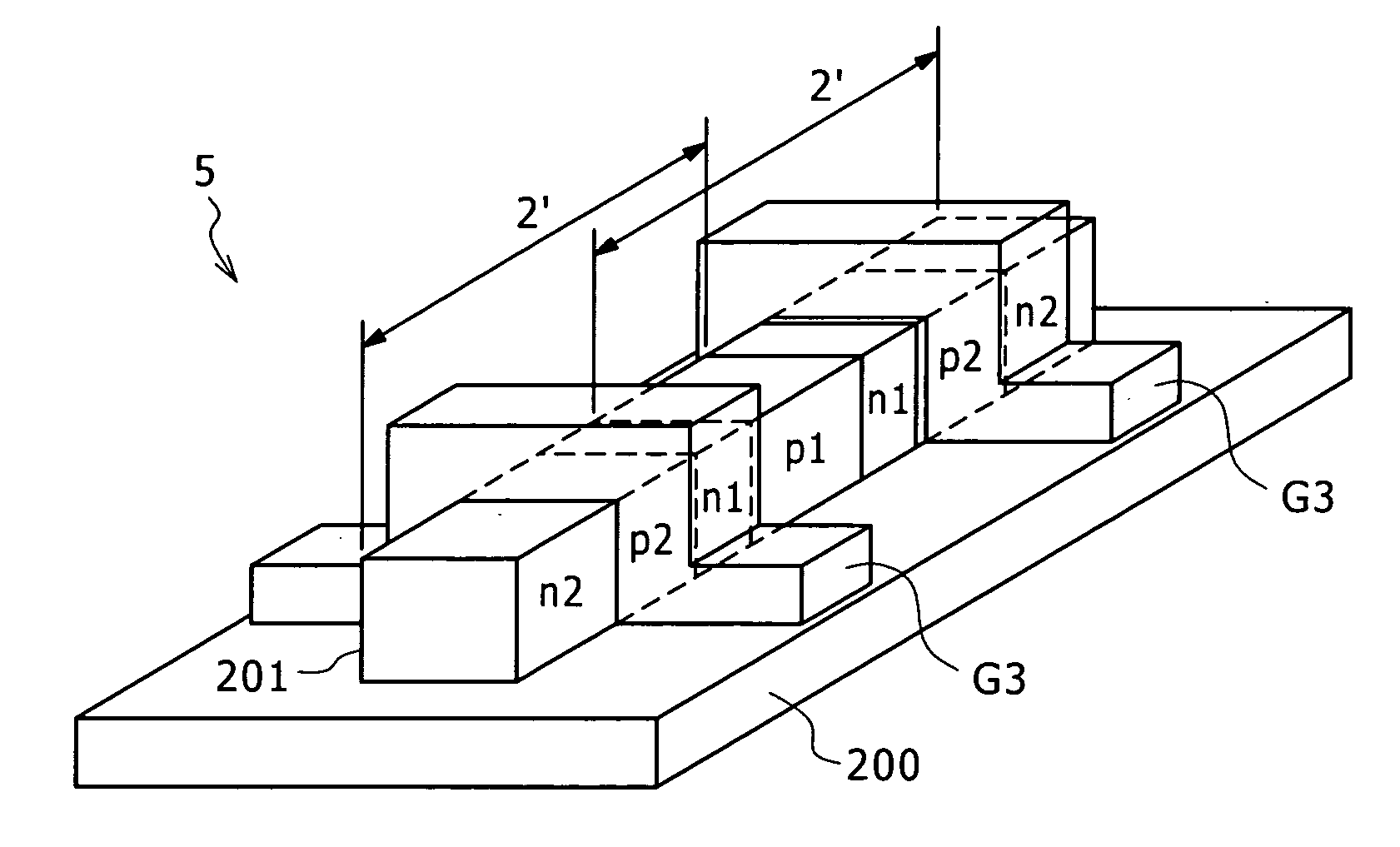
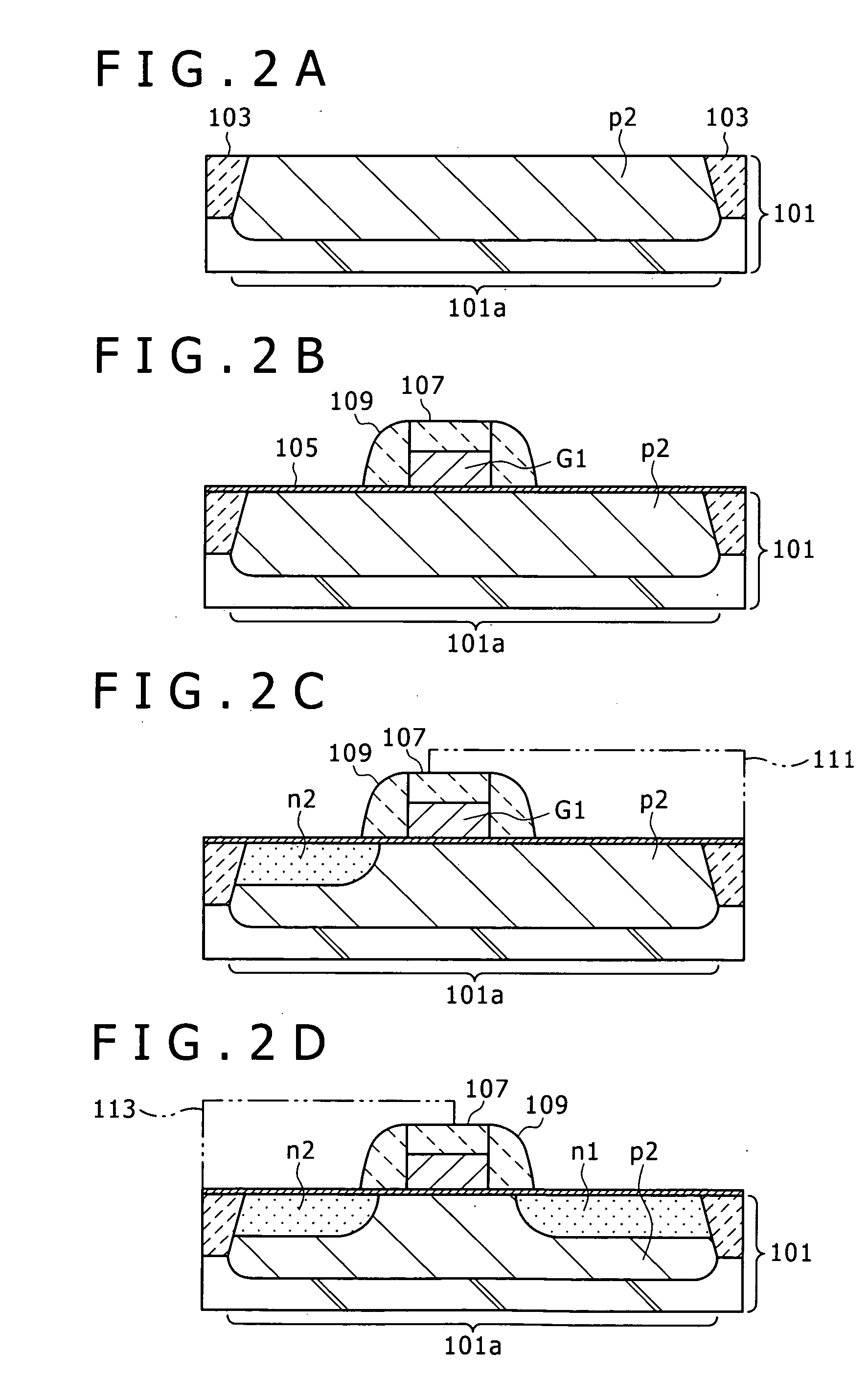
[0076] A method for manufacturing the semiconductor device 2 of the second embodiment will be described below with reference to step diagrams of FIGS. 4A to 4F.

[0077] Referring initially to FIG. 4A, a semiconductor thin film 201a formed on the insulating film 200 of an SOI substrate is patterned into a ridge shape extending in one direction, to thereby form the semiconductor layer 201 processed into a three-dimensional fin structure. The semiconductor layer 201 serves as an active region.

[0078] Subsequently, the p-region p2 is formed in the entire semiconductor layer 201 through ion implantation. In this ion implantation, the p-type dopant to be introduced for the p-region p2 is e.g. boron (B), and the dose thereof is e.g. 5E18 / cm3, and is preferably about 1E18 to 1E19 / cm3. The p-type dopant may be indium (In).

[0079] Subsequently, the formation of a sacrificial oxide film for eliminating damage on the semiconductor layer 201 and etch-removal of the sacrificial oxide film are carri...

fourth embodiment

[0102] After the above-described step, the insulating film 401 over the offset insulating film 301 and the sidewall 203 are removed by polishing according to need. Alternatively, the insulating film 401 and the sidewall may be left if they are used as interlayer insulating films. In addition, contact holes to the gate electrodes G1′ and G2′, the p-region p1 and the n-region n2 are opened and metal interconnects are provided although not illustrated in the drawings, so that the semiconductor device 4 of the fourth embodiment described with FIG. 6 can be completed.

[0103] In the semiconductor devices of the first to fourth embodiments, the p-region p2 is provided with a gate electrode. However, semiconductor devices of embodiments of the invention may have a structure in which the n-region n1 in an intermediate area is provided with a gate electrode.

[0104] In the manufacturing of the semiconductor devices of the first to fourth embodiments, the formation order of the p-region p1 and t...


PUM


Abstract

The present invention is to provide a semiconductor device including: a semiconductor layer that has a first-conductivity-type region, a second-conductivity-type region, a first-conductivity-type region, and a second-conductivity-type region that are adjacent to each other in that order; first and second electrodes that are connected to the first-conductivity-type region and the second-conductivity-type region, respectively, at both ends of the semiconductor layer; and a gate electrode that is coupled to the second-conductivity-type region or the first-conductivity-type region in an intermediate area of the semiconductor layer, the gate electrode being provided over a plurality of faces of a semiconductor layer portion serving as the second-conductivity-type region or the first-conductivity-type region in the intermediate area.

Description

CROSS REFERENCES TO RELATED APPLICATIONS [0001] The present invention contains subject matter related to Japanese Patent Application JP 2005-206400 filed with the Japanese Patent Office on Jul. 15, 2005 and Japanese Patent Application JP 2006-047652 filed with the Japanese Patent Office on Feb. 24, 2006, the entire contents of which being incorporated herein by reference. BACKGROUND OF THE INVENTION [0002] 1. Field of the Invention [0003] The present invention relates to a thyristor-based semiconductor device and a method for manufacturing the semiconductor device. [0004] 2. Description of the Related Art [0005] As shown in FIG. 15A, in a general thyristor-based semiconductor device, four layers of p-type regions (hereinafter, p-regions) p1 and p2 and n-type regions (hereinafter, n-regions) n1 and n2 are formed in such a manner that the p- and n-regions are in turn arranged to construct a p1 / n1 / p2 / n2 structure. Furthermore, an anode electrode A is connected to the p-region p1 at one...

Claims


Application Information

Patent Timeline
IPC IPC(8): H01L29/74H01L21/332
CPCH01L21/84H01L27/108H01L27/10826H01L27/11H01L27/1104H01L29/87H01L29/0657H01L29/7391H01L29/785H01L29/78648H01L27/1203H10B12/36H10B12/00H10B10/00H10B10/12
Inventor SUGIZAKI, TARO
Owner SONY CORP
Why Eureka
Try Eureka