Semiconductor Memory

a technology of semiconductor devices and memory cells, applied in semiconductor devices, digital storage, instruments, etc., can solve the problems of limitation of conventional memory cells in implementing high-speed performance of cells, and achieve the effect of preventing the occurrence of read disturbances

Inactive Publication Date: 2007-09-20
RENESAS ELECTRONICS CORP
View PDF5 Cites 31 Cited by
  • Summary
  • Abstract
  • Description
  • Claims
  • Application Information

AI Technical Summary

Benefits of technology

[0011] The present invention provides a phase-change memory including a selection transistor and chalcogenide. During the data reading, a maximum voltage indicating a threshold voltage can be applied to the selection transistor, such that data can be read at high speed. Also, the record voltage can be higher than the withstanding voltage of the selection transistor, such that a margin between the read and record voltages can be sufficiently guaranteed, resulting in the prevention of the occurrence of read disturbance. As a result, a non-volatile memory of high-reliability and high-performance is implemented. Specifically, the present invention can be effectively applied to a system LSI including the non-volatile memories.

Problems solved by technology

In other words, in the case of conventional memory cells, the implementation of the high-speed cell and the prevention of read disturbance are traded off, such that the conventional memory cells have limitation in implementing the high-speed performance of the cell.

Method used


Image

  • Semiconductor Memory
  • Semiconductor Memory
  • Semiconductor Memory

Examples


first preferred embodiment

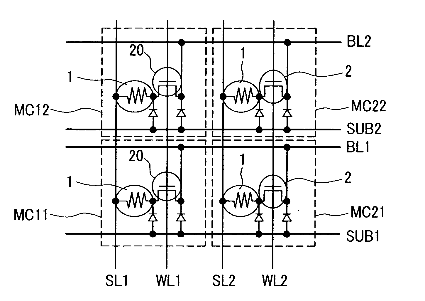
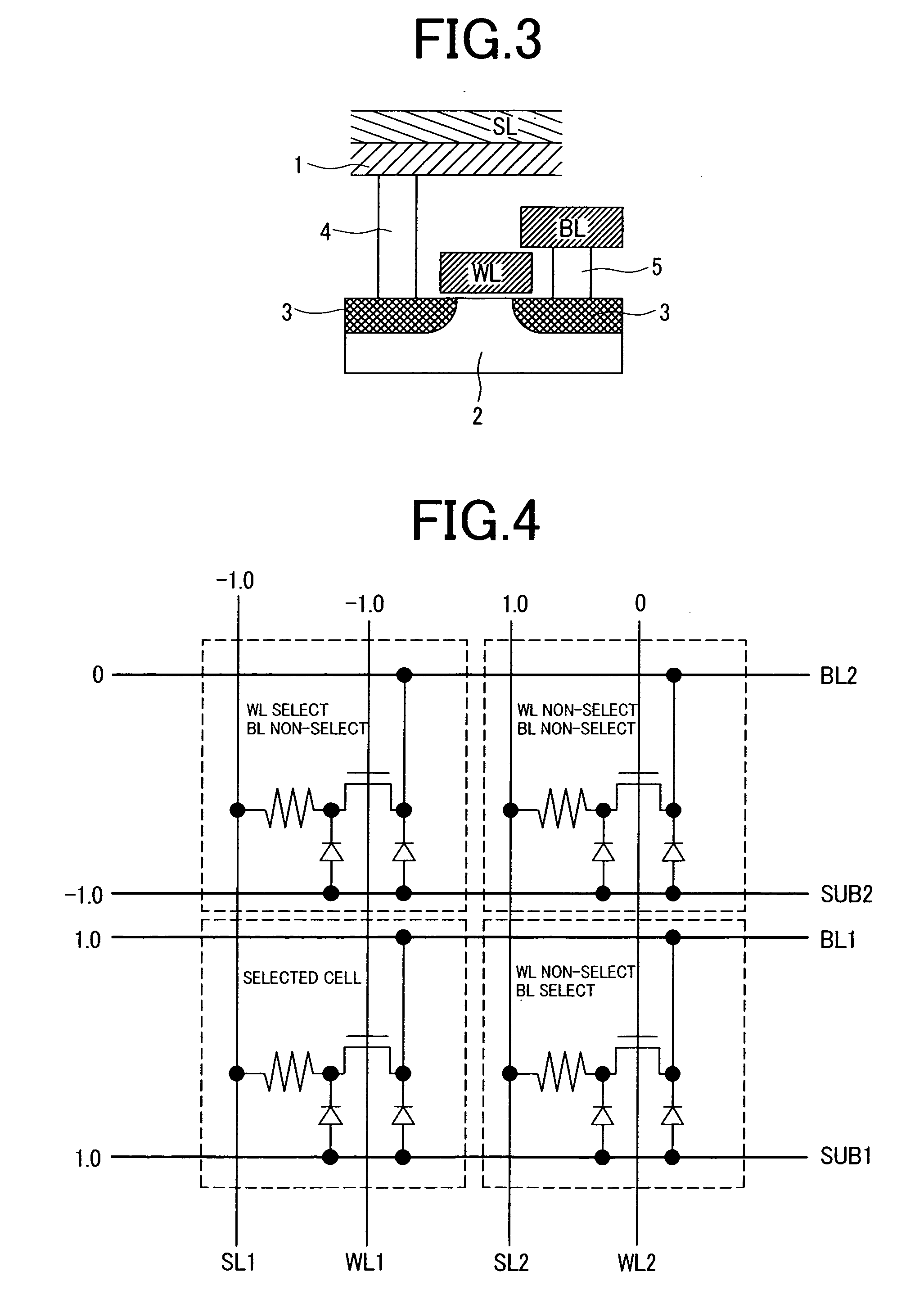
[0051]FIG. 1 is a structural diagram illustrating a memory array according to the present invention. A method for fabricating a memory array of FIG. 1 will hereinafter be described according to a fabrication process of the memory array. FIG. 1 shows only the memory array. An isolation layer 6 is formed as shown in FIG. 5. FIG. 5 is a top view illustrating a fabrication process of a semiconductor memory according to a first preferred embodiment of the present invention. In order to form the isolation layer 6, a trench groove is formed in a silicon substrate by general photolithography and dry-etching processes. A CMOS well is formed by a general fabrication method. An N-type well is formed in a memory array. In order to implement the memory array of FIG. 1, a substrate potential of the cell array is separated in the direction parallel to a bit line. For this purpose, only the memory array is exposed by the general photolithography, and a p-type diffusion layer 8 is deposited under th...

second preferred embodiment

[0072] The second preferred embodiment of the present invention relates to a method for implementing a phase-change memory array having superior noise resistance. For this purpose, the second preferred embodiment of the present invention employs a folded bit-line arrangement (i.e., a memory array including two intersection points) widely used for DRAMs. A fabrication process of the second preferred embodiment is almost similar to that of the first preferred embodiment. Also, the second preferred embodiment also uses a method for isolating each component using a gate electrode in the same manner as in the first preferred embodiment. The fabrication method of the second preferred embodiment will hereinafter be described with reference to the annexed drawings. A method for isolating each component, a method for forming a word-line electrode, and a method for forming an impurity diffusion layer of the second preferred embodiment are equal to those of the first preferred embodiment, and ...

third preferred embodiment

[0075] The first and second preferred embodiments have isolated each component by a combination of a shallow trench isolation and a field plate isolation. The third preferred embodiment employs only the shallow trench isolation. The third preferred embodiment does not use a gate electric field for isolation of each component, such that it can easily control a word system, and a detailed description thereof will hereinafter be described. N-type well is formed in the memory cell array using a P-type substrate. An isolation layer shown in FIG. 26 is formed by a typical CMOS process. Next, in order to isolate a substrate potential in a direction parallel to a bit line, a resist pattern of FIG. 27 is used as a mask, and implantation of P-type impurity is executed. FIG. 28 is a cross-sectional view illustrating a semiconductor memory taken along the line A-A of FIG. 27. A diffusion layer must be thicker than the isolation layer 6, differently from the example of FIG. 6. The remaining part...


PUM


Abstract

A phase-change memory for employing chalcogenide as a recording medium is disclosed, which prevents the read disturbance from being generated, and reads data at high speed. In a phase-change memory cell array including a selection transistor and chalcogenide, a substrate potential of the selection transistor is isolated in a direction perpendicular to the word lines. During the data recording, a forward current signal flows between the substrate and the source line connected to chalcogenide, and the selection transistor is not used. During the data reading, a desired cell is selected by the selection transistor. Therefore, a recording voltage is greatly higher than the reading voltage, such that the occurrence of read disturbance is prevented, and a high-speed operation is implemented.

Description

TECHNICAL FIELD [0001] The present invention relates to a semiconductor memory, and more particularly to a non-volatile random access memory (RAM) operated at low voltage at high speed. BACKGROUND ART [0002] With the increasing demands of mobile devices such as mobile phones, non-volatile memories and associated technology are being rapidly researched by many developers throughout the world. A representative example of the non-volatile memory is a flash memory. The flash memory is operated at low speed, such that it has been widely used as a programmable ROM. [0003] In the meantime, a high-speed DRAM is required for an operation memory. A memory for portable or mobile devices includes not only the flash memory but also the DRAM. If a semiconductor device including characteristics of the above-mentioned two memories (i.e., the flash memory and the DRAM) can be implemented, the flash memory and the DRAM can be integrated into a single chip, and this integrated chip can substitute for ...

Claims


Application Information

Patent Timeline
Patent Type & Authority Applications(United States)
IPC IPC(8): G11C11/00G11C13/00G11C16/02G11C16/10H01L27/10H01L27/24
CPCG11C13/0004G11C13/003G11C13/0069G11C2213/72G11C2213/74G11C2213/76H01L27/2463H01L27/101H01L45/06H01L45/1233H01L45/144H01L45/1675H01L27/2436G11C2213/79H10B63/30H10B63/80H10N70/231H10N70/826H10N70/8828H10N70/063
Inventor MATSUOKA, HIDEYUKITAKEMURA, RIICHIRO
Owner RENESAS ELECTRONICS CORP
Why Eureka
Try Eureka