Image forming apparatus and semiconductor laser modulation driving apparatus

a technology of semiconductor laser and driving apparatus, which is applied in the field of semiconductor laser, can solve the problems of complex configuration required for signal transfer and high-speed signal transfer may be actually difficult, so as to reduce the swing of signal input and reduce the fluctuation of current source. , the effect of high-speed signal transmission

Inactive Publication Date: 2005-04-28
RICOH KK
View PDF24 Cites 53 Cited by
  • Summary
  • Abstract
  • Description
  • Claims
  • Application Information

AI Technical Summary

Benefits of technology

[0021] (6) Also, it is possible to apply a desired low swing output as output of the semiconductor laser modulation signal generating part. Also, high speed signal transmission is achieved.
[0022] (7) Further, it is possible to reduce swing of a signal input to a CML circuit, to reduce a fluctuation of a current source possibly occurring due to switching in the CML circuit, and thus to increase a switching speed therein.
[0023] (8) Since it is possible to obtain a low swing differential signal from a single LD modulation signal, it is possible to achieve data transfer at a high speed with a high definition.
[0024] (9) In a case where a resistor or a resistance in an integrated circuit is applied as a load of a CML circuit, a variation in output swing possibly occurring due to a variation of the resistor or resistance is reduced, and thus, it is possible to achieve output with precise swing.
[0025] (10) In a case where an external resistor or a resistance is applied as a load of a CML circuit, also a variation in output swing possibly occurring due to a variation in the resistor or resistance is reduced, and thus, it is possible to achieve output with precise swing.
[0026] (11) Also in a multi-beam image forming apparatus or a tandem type image forming apparatus, high speed data transfer is achieved.

Problems solved by technology

However, in such a configuration, since the number of signal lines required is large, a configuration required for the signal transfer becomes complicated, and a high speed signal transfer may be actually difficult.

Method used


Image

  • Image forming apparatus and semiconductor laser modulation driving apparatus
  • Image forming apparatus and semiconductor laser modulation driving apparatus
  • Image forming apparatus and semiconductor laser modulation driving apparatus

Examples


first embodiment

[0077] the present invention is described.

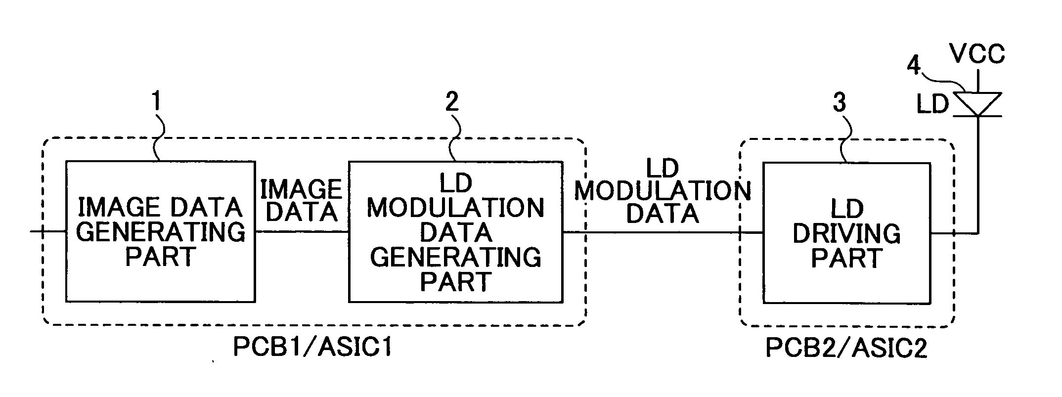
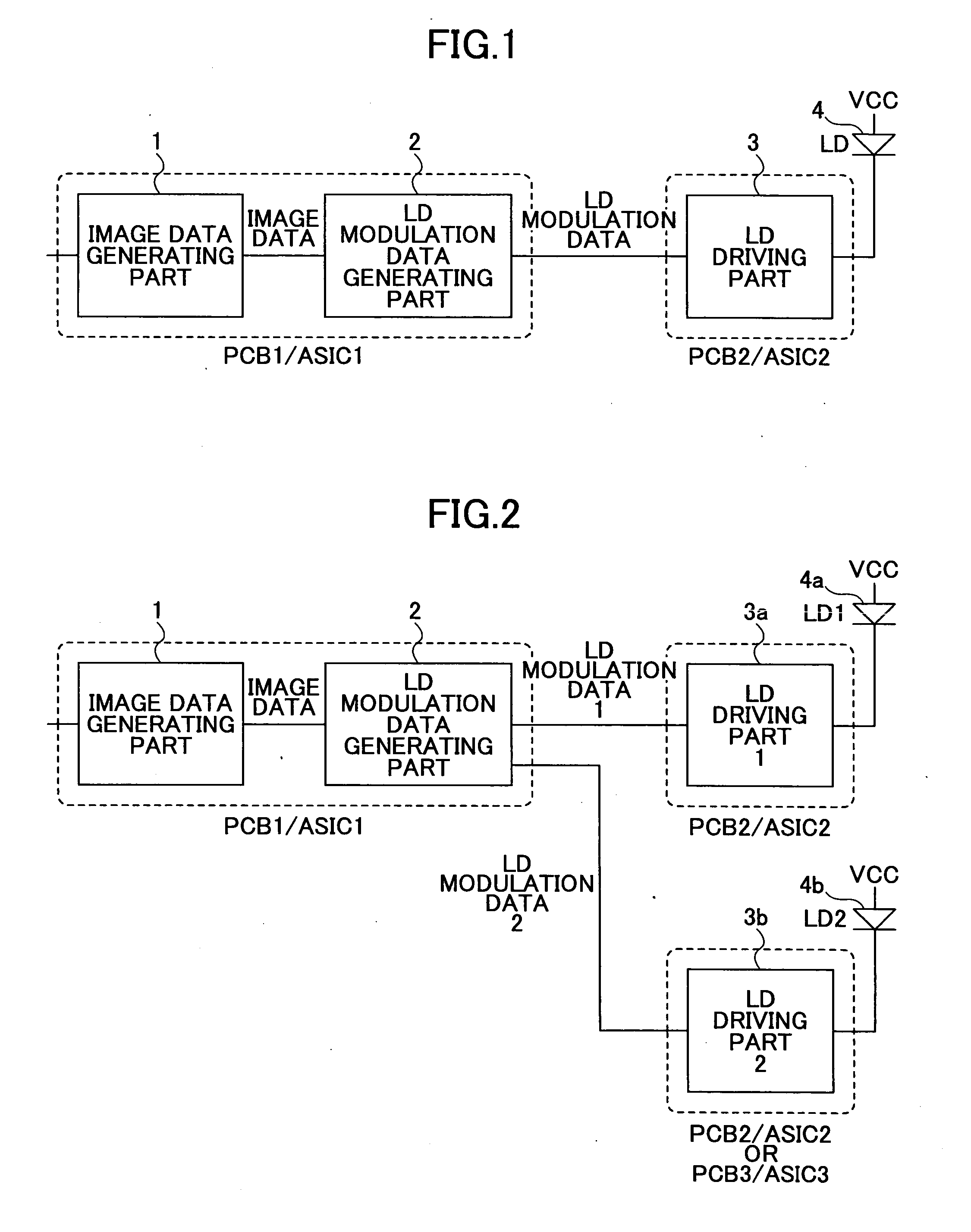
[0078]FIG. 1 shows a first configuration according to the first embodiment of the present invention. As shown in FIG. 1, the configuration includes an image data generating part 1, an LD modulation data generating part 2. an LD driving part 3, and an LD 4. In this configuration, the image data generating part 1 and the LD modulation signal generating part 2 are configured in a common single substrate PCB1 or a common single ASIC1, while the LD driving part 3 is disposed closely to the LD 4. As the number of channels increases in LDs and color image forming is widely spread, the number of signals for image data further increases. In order to properly respond to such increase in the number of signal lines for image data, it is advantageous to provide the image data generating part 1 and the LD modulation data generating part 2 on a same substrate, or, to provide the functions thereof within a same ASIC, and thereby, a plurality of signals can ...

second embodiment

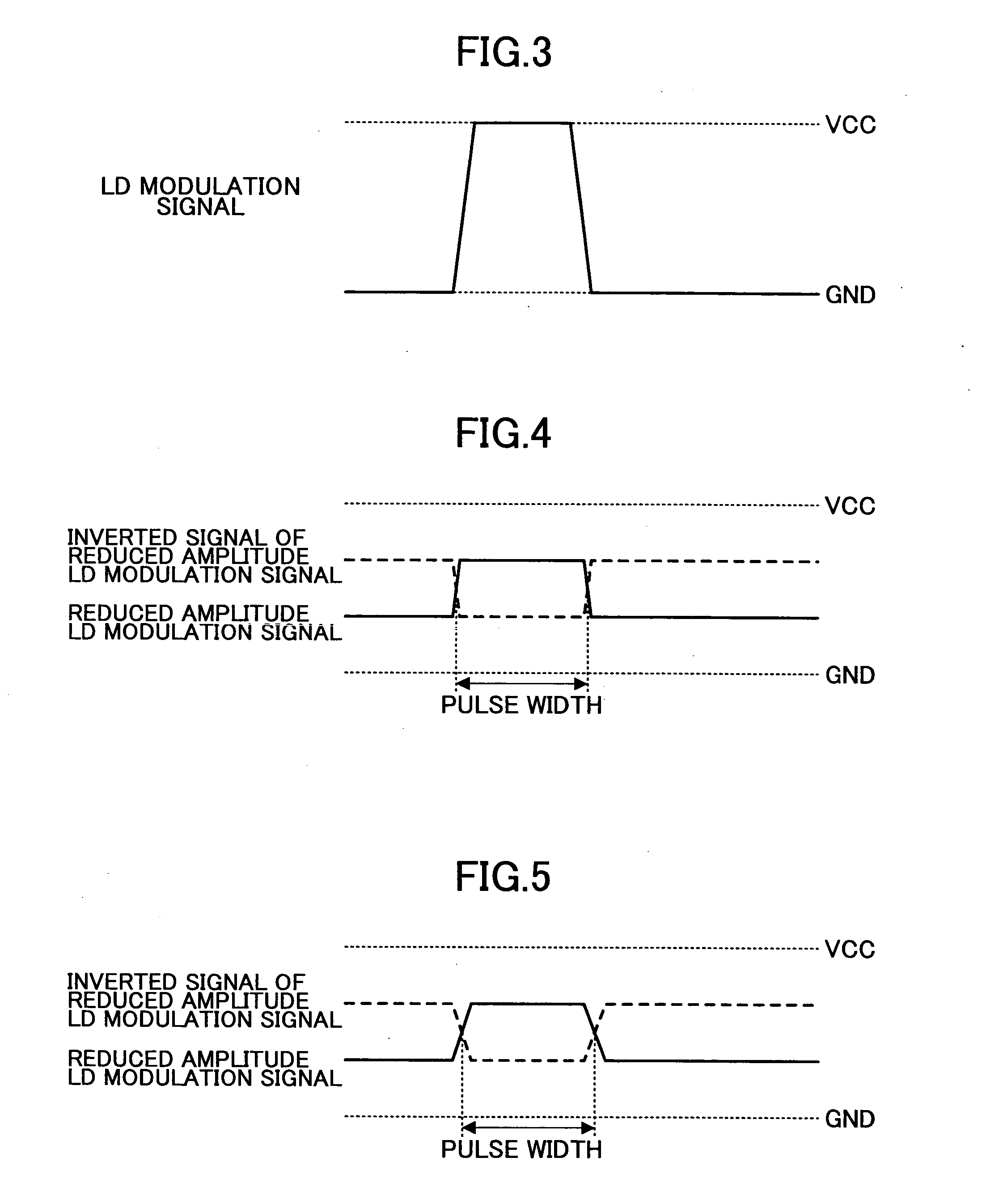
[0093] A method for generating the above-mentioned reduced amplitude differential signal according to the present invention is described next. Although a part outputting the reduced amplitude differential signal described now is configured in a single stage of an inverter, the present invention may also be applied to a configuration in which the part outputting the reduced amplitude differential signal is configured by a plurality of stages of inverters or buffers, instead.

[0094]FIG. 15 shows a first configuration according to the second embodiment of the present invention. In this configuration, a differential signal is input to a CML circuit CML, and resistors (or resistances) R1 and R2 are applied as loads of the CML circuit CML. In this configuration, it is possible to reduce output amplitude of the CML circuit CML to be smaller than VCC. Further, by adjusting values of the resistors (or resistances) R1 and R2, the output amplitude can be controlled.

[0095]FIG. 16 shows a second...

third embodiment

[0118] the present invention is described next.

[0119]FIG. 38 shows a configuration of semiconductor laser modulation signal generating parts and semiconductor laser driving parts in a tandem-type color machine in the related art. In this configuration, a semiconductor laser modulation signal generating part 100 and a semiconductor laser driving part 200 are provided for each of the respective color components, i.e., yellow (Y), magenta (M), cyan (C) and black (K). In this configuration, a reference clock signal is adjustable for each color component, and thus, the configuration is superior in terms of versatility. In the configuration of FIG. 38, the semiconductor laser modulation signal generating part 100 may have a configuration which includes the LD modulation data generating part 2 shown in FIG. 1 or such; includes both the image data generating part 1 and the LD modulation data generating part 2 as shown in FIG. 1 or such; or includes both the image data generating part 1 and ...


PUM


Abstract

A color image forming apparatus produces a latent image on a photosensitive body based on a signal output from a scanning light detecting part in response to detection of scanning light; a semiconductor laser modulation signal generating part includes a clock generating part and a clock modulation part; a semiconductor laser and a semiconductor laser driving part are provided for each color of yellow, magenta, cyan and black; and further, a plurality of the semiconductor lasers are provided for at least one color of yellow, magenta, cyan and black.

Description

BACKGROUND OF THE INVENTION [0001] 1. Field of the Invention [0002] The present invention relates to a semiconductor laser (simply referred to as an ‘LD’, hereinafter) modulation signal generating circuit and an image forming apparatus, and, in particular, to an LD modulation signal generating circuit modulating light output of a light source in a laser printer, an optical disk apparatus, a digital copier, an optical communication apparatus or such, and a semiconductor laser modulating apparatus and an image forming apparatus modulating light output of the light source and forming an image in the laser printer, optical disk apparatus, digital copier, optical communication apparatus or such. [0003] 2. Description of the Related Art [0004] In a laser printer, an optical disk apparatus, a digital copier, an optical communication apparatus or such, in order to modulate light output of a light source, an image data generating part, an LD modulation data generating part and an LD driver a...

Claims


Application Information

Patent Timeline
Patent Type & Authority Applications(United States)
IPC IPC(8): B41J2/44G06K15/12H04N1/04H04N1/113H04N1/23
CPCG06K15/129
Inventor OZASA, DANISHIDA, MASAAKINIHEI, YASUHIROOMORI, ATSUFUMI
Owner RICOH KK
Why Eureka
Try Eureka